Home > Press > Berkeley Lab Researchers Create Nanoscale Waveguide for Future Photonics
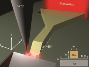 |
| The hybrid plasmon polariton (HPP) nanoscale waveguide consists of a semiconductor strip separated from a metallic surface by a low dielectric gap. Schematic shows HPP waveguide responding when a metal slit at the guide�s input end is illuminated. (courtesy of Zhang group) |
Abstract:
The creation of a new quasiparticle called the "hybrid plasmon polariton" may throw open the doors to integrated photonic circuits and optical computing for the 21st century. Researchers with the U.S. Department of Energy (DOE)'s Lawrence Berkeley National Laboratory (Berkeley Lab) have demonstrated the first true nanoscale waveguides for next generation on-chip optical communication systems.
Berkeley Lab Researchers Create Nanoscale Waveguide for Future Photonics
Berkeley, CA | Posted on June 1st, 2011"We have directly demonstrated the nanoscale waveguiding of light at visible and near infrared frequencies in a metal-insulator-semiconductor device featuring low loss and broadband operation," says Xiang Zhang, the leader of this research. "The novel mode design of our nanoscale waveguide holds great potential for nanoscale photonic applications, such as intra-chip optical communication, signal modulation, nanoscale lasers and bio-medical sensing."
Zhang, a principal investigator with Berkeley Lab's Materials Sciences Division and director of the University of California at Berkeley's Nano-scale Science and Engineering Center (SINAM), is the corresponding author of a paper published by Nature Communications that describes this work titled "Experimental Demonstration of Low-Loss Optical Waveguiding at Deep Sub-wavelength Scales." Co-authoring the paper with Zhang were Volker Sorger, Ziliang Ye, Rupert Oulton, Yuan Wang, Guy Bartal and Xiaobo Yin.
In this paper, Zhang and his co-authors describe the use of the hybrid plasmon polariton, a quasi-particle they conceptualized and created, in a nanoscale waveguide system that is capable of shepherding light waves along a metal-dielectric nanostructure interface over sufficient distances for the routing of optical communication signals in photonic devices. The key is the insertion of a thin low-dielectric layer between the metal and a semiconductor strip.
"We reveal mode sizes down to 50-by-60 square nanometers using Near-field scanning optical microscopy (NSOM) at optical wavelengths," says Volker Sorger a graduate student in Zhang's research group and one of the two lead authors on the Nature Communications paper. "The propagation lengths were 10 times the vacuum wavelength of visible light and 20 times that of near infrared."
The high-technology world is eagerly anticipating the replacement of today's electronic circuits in microprocessors and other devices with circuits based on the transmission of light and other forms of electromagnetic waves. Photonic technology, or "photonics," promises to be superfast and ultrasensitive in comparison to electronic technology.
"To meet the ever-growing demand for higher data bandwidth and lower power consumption, we need to reduce the energy required to create, transmit and detect each bit of information," says Sorger. "This requires reducing physical photonic component sizes down beyond the diffraction limit of light while still providing integrated functionality."
Until recently, the size and performance of photonic devices was constrained by the interference that arises between closely spaced light waves. This diffraction limit results in weak photonic-electronic interactions that can only be avoided through the use of devices much larger in size than today's electronic circuits. A breakthrough came with the discovery that it is possible to couple photons with electrons by squeezing light waves through the interface between a metal/dielectric nanostructure whose dimensions are smaller than half the wavelengths of the incident photons in free space.
Directing waves of light across the surface of a metal nanostructure generates electronic surface waves - called plasmons - that roll through the metal's conduction electrons (those loosely attached to molecules and atoms). The resulting interaction between plasmons and photons creates a quasi-particle called a surface plasmon polariton(SPP) that can serve as a carrier of information. Hopes were high for SPPs in nanoscale photonic devices because their wavelengths can be scaled down below the diffraction limit, but problems arose because any light signal loses strength as it passes through the metal portion of a metal-dielectric interface.
"Until now, the direct experimental demonstration of low-loss propagation of deep sub-wavelength optical modes was not realized due to the huge propagation loss in the optical mode that resulted from the electromagnetic field being pushed into the metal," Zhang says. "With this trade-off between optical confinement and metallic losses, the use of plasmonics for integrated photonics, in particular for optical interconnects, has remained uncertain."
To solve the problem of optical signal loss, Zhang and his group proposed the hybrid plasmon polariton (HPP) concept. A semiconductor (high-dielectric) strip is placed on a metal interface, just barely separated by a thin oxide (low-dielectric) layer. This new metal-oxide-semiconductor design results in a redistribution of an incoming light wave's energy. Instead of being concentrated in the metal, where optical losses are high, some of the light wave's energy is squeezed into the low dielectric gap where optical losses are substantially less compared to the plasmonic metal.
"With this design, we create an HPP mode, a hybrid of the photonic and plasmonic modes that takes the best from both systems and gives us high confinement with low signal loss," says Ziliang Ye, the other lead authors of the Nature Communications paper who is also a graduate student in Zhang's research group. "The HPP mode is not only advantageous for down-scaling physical device sizes, but also for delivering novel physical effects at the device level that pave the way for nanolasers, as well as for quantum photonics and single-photon all-optical switches."
The HPP waveguide system is fully compatible with current semiconductor/CMOS processing techniques, as well as with the Silicon-on-Insulator (SOI) platform used today for photonic integration. This should make it easier to incorporate the technology into low-cost, large-scale integration and manufacturing schemes. Sorger believes that prototypes based on this technology could be ready within the next two years and the first actual products could be on the market within five years.
"We are already working on demonstrating an all-optical transistor and electro-optical modulator based on the HPP waveguide system," Sorger says. "We're also now looking into bio-medical applications, such as using the HPP waveguide to make a molecular sensor."
This research was supported by the National Science Foundation's Nano-Scale Science and Engineering Center.
####
About Berkeley Lab
Lawrence Berkeley National Laboratory addresses the world�s most urgent scientific challenges by advancing sustainable energy, protecting human health, creating new materials, and revealing the origin and fate of the universe. Founded in 1931, Berkeley Lab�s scientific expertise has been recognized with 12 Nobel prizes. The University of California manages Berkeley Lab for the U.S. Department of Energy�s Office of Science. For more, visit www.lbl.gov.
For more information, please click here
Contacts:
Lynn Yarris
(510) 486-5375
Copyright © Berkeley Lab
If you have a comment, please Contact us.Issuers of news releases, not 7th Wave, Inc. or Nanotechnology Now, are solely responsible for the accuracy of the content.
Bookmark:


| Related Links |
![]() For more information about the research of Xiang Zhang visit:
For more information about the research of Xiang Zhang visit:
| Related News Press |
News and information
![]() Simulating magnetization in a Heisenberg quantum spin chain April 5th, 2024
Simulating magnetization in a Heisenberg quantum spin chain April 5th, 2024
![]() NRL charters Navy�s quantum inertial navigation path to reduce drift April 5th, 2024
NRL charters Navy�s quantum inertial navigation path to reduce drift April 5th, 2024
![]() Discovery points path to flash-like memory for storing qubits: Rice find could hasten development of nonvolatile quantum memory April 5th, 2024
Discovery points path to flash-like memory for storing qubits: Rice find could hasten development of nonvolatile quantum memory April 5th, 2024
Laboratories
![]() A battery�s hopping ions remember where they�ve been: Seen in atomic detail, the seemingly smooth flow of ions through a battery�s electrolyte is surprisingly complicated February 16th, 2024
A battery�s hopping ions remember where they�ve been: Seen in atomic detail, the seemingly smooth flow of ions through a battery�s electrolyte is surprisingly complicated February 16th, 2024
![]() NRL discovers two-dimensional waveguides February 16th, 2024
NRL discovers two-dimensional waveguides February 16th, 2024
![]() Three-pronged approach discerns qualities of quantum spin liquids November 17th, 2023
Three-pronged approach discerns qualities of quantum spin liquids November 17th, 2023
Govt.-Legislation/Regulation/Funding/Policy
![]() NRL charters Navy�s quantum inertial navigation path to reduce drift April 5th, 2024
NRL charters Navy�s quantum inertial navigation path to reduce drift April 5th, 2024
![]() Discovery points path to flash-like memory for storing qubits: Rice find could hasten development of nonvolatile quantum memory April 5th, 2024
Discovery points path to flash-like memory for storing qubits: Rice find could hasten development of nonvolatile quantum memory April 5th, 2024
![]() Chemical reactions can scramble quantum information as well as black holes April 5th, 2024
Chemical reactions can scramble quantum information as well as black holes April 5th, 2024
Discoveries
![]() Chemical reactions can scramble quantum information as well as black holes April 5th, 2024
Chemical reactions can scramble quantum information as well as black holes April 5th, 2024
![]() New micromaterial releases nanoparticles that selectively destroy cancer cells April 5th, 2024
New micromaterial releases nanoparticles that selectively destroy cancer cells April 5th, 2024
![]() Utilizing palladium for addressing contact issues of buried oxide thin film transistors April 5th, 2024
Utilizing palladium for addressing contact issues of buried oxide thin film transistors April 5th, 2024
Announcements
![]() NRL charters Navy�s quantum inertial navigation path to reduce drift April 5th, 2024
NRL charters Navy�s quantum inertial navigation path to reduce drift April 5th, 2024
![]() Discovery points path to flash-like memory for storing qubits: Rice find could hasten development of nonvolatile quantum memory April 5th, 2024
Discovery points path to flash-like memory for storing qubits: Rice find could hasten development of nonvolatile quantum memory April 5th, 2024
Photonics/Optics/Lasers
![]() With VECSELs towards the quantum internet Fraunhofer: IAF achieves record output power with VECSEL for quantum frequency converters April 5th, 2024
With VECSELs towards the quantum internet Fraunhofer: IAF achieves record output power with VECSEL for quantum frequency converters April 5th, 2024
![]() Nanoscale CL thermometry with lanthanide-doped heavy-metal oxide in TEM March 8th, 2024
Nanoscale CL thermometry with lanthanide-doped heavy-metal oxide in TEM March 8th, 2024
![]() Optically trapped quantum droplets of light can bind together to form macroscopic complexes March 8th, 2024
Optically trapped quantum droplets of light can bind together to form macroscopic complexes March 8th, 2024
![]() HKUST researchers develop new integration technique for efficient coupling of III-V and silicon February 16th, 2024
HKUST researchers develop new integration technique for efficient coupling of III-V and silicon February 16th, 2024
|
|
||
|
|
||
| The latest news from around the world, FREE | ||
|
|
||
|
|
||
| Premium Products | ||
|
|
||
|
Only the news you want to read!
Learn More |
||
|
|
||
|
Full-service, expert consulting
Learn More |
||
|
|
||