Home > Press > Stamping Out Low Cost Nanodevices
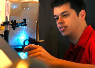 |
| Anne Raynor, Vanderbilt University
Vanderbilt graduate student Jason Ryckman demonstrates operation of a biosensor made from nanoporous materials. |
Abstract:
A simple technique for stamping patterns invisible to the human eye onto a special class of nanomaterials provides a new, cost-effective way to produce novel devices in areas ranging from drug delivery to solar cells.
Stamping Out Low Cost Nanodevices
Nashville, TN | Posted on June 1st, 2011The technique was developed by Vanderbilt University engineers and described in the cover article of the May issue of the journal Nano Letters.
The new method works with materials that are riddled with tiny voids that give them unique optical, electrical, chemical and mechanical properties. Imagine a stiff, sponge-like material filled with holes that are too small to see without a special microscope.
For a number of years, scientists have been investigating the use of these materials - called porous nanomaterials - for a wide range of applications including drug delivery, chemical and biological sensors, solar cells and battery electrodes. There are nanoporous forms of gold, silicon, alumina, and titanium oxide, among others.
Simple stamping
A major obstacle to using the materials has been the complexity and expense of the processing required to make them into devices.
Now, Associate Professor of Electrical Engineering Sharon M. Weiss and her colleagues have developed a rapid, low-cost imprinting process that can stamp out a variety of nanodevices from these intriguing materials.
"It's amazing how easy it is. We made our first imprint using a regular tabletop vise," Weiss said. "And the resolution is surprisingly good."
The traditional strategies used for making devices out of nanoporous materials are based on the process used to make computer chips. This must be done in a special clean room and involves painting the surface with a special material called a resist, exposing it to ultraviolet light or scanning the surface with an electron beam to create the desired pattern and then applying a series of chemical treatments to either engrave the surface or lay down new material. The more complicated the pattern, the longer it takes to make.
About two years ago, Weiss got the idea of creating pre-mastered stamps using the complex process and then using the stamps to create the devices. Weiss calls the new approach direct imprinting of porous substrates (DIPS). DIPS can create a device in less than a minute, regardless of its complexity. So far, her group reports that it has used master stamps more than 20 times without any signs of deterioration.
Process can produce nanoscale patterns
The smallest pattern that Weiss and her colleagues have made to date has features of only a few tens of nanometers, which is about the size of a single fatty acid molecule. They have also succeeded in imprinting the smallest pattern yet reported in nanoporous gold, one with 70-nanometer features.
The first device the group made is a "diffraction-based" biosensor that can be configured to identify a variety of different organic molecules, including DNA, proteins and viruses. The device consists of a grating made from porous silicon treated so that a target molecule will stick to it. The sensor is exposed to a liquid that may contain the target molecule and then is rinsed off. If the target was present, then some of the molecules stick in the grating and alter the pattern of reflected light produced when the grating is illuminated with a laser.
According to the researchers' analysis, when such a biosensor is made from nanoporous silicon it is more sensitive than those made from ordinary silicon.
The Weiss group collaborated with colleagues in Chemical and Biomolecular Engineering to use the new technique to make nano-patterned chemical sensors that are ten times more sensitive than another type of commercial chemical sensor called Klarite that is the basis of a multimillion-dollar market.
The researchers have also demonstrated that they can use the stamps to make precisely shaped microparticles by a process called "over-stamping" that essentially cuts through the nanoporous layer to free the particles from the substrate. One possible application for microparticles made this way from nanoporous silicon are as anodes in lithium-ion batteries, which could significantly increase their capacity without adding a lot of weight.
Vanderbilt University has applied for a patent on the DIPS method.
Vanderbilt graduate student Judson D. Ryckman, Marco Liscidini, University of Pavia and John E. Sipe, University of Toronto, contributed to the research, which was supported by grants from the U.S. Army Research Office, INNESCO project, The National Sciences and Engineering Research Council of Canada and a Graduate Research Fellowship from the National Science Foundation.
Visit Research News @ Vanderbilt for more research news from Vanderbilt.
####
For more information, please click here
Contacts:
David F. Salisbury
(615) 322-NEWS
Copyright © Newswise
If you have a comment, please Contact us.Issuers of news releases, not 7th Wave, Inc. or Nanotechnology Now, are solely responsible for the accuracy of the content.
Bookmark:


| Related News Press |
News and information
![]() Simulating magnetization in a Heisenberg quantum spin chain April 5th, 2024
Simulating magnetization in a Heisenberg quantum spin chain April 5th, 2024
![]() NRL charters Navy�s quantum inertial navigation path to reduce drift April 5th, 2024
NRL charters Navy�s quantum inertial navigation path to reduce drift April 5th, 2024
![]() Discovery points path to flash-like memory for storing qubits: Rice find could hasten development of nonvolatile quantum memory April 5th, 2024
Discovery points path to flash-like memory for storing qubits: Rice find could hasten development of nonvolatile quantum memory April 5th, 2024
Chemistry
![]() What heat can tell us about battery chemistry: using the Peltier effect to study lithium-ion cells March 8th, 2024
What heat can tell us about battery chemistry: using the Peltier effect to study lithium-ion cells March 8th, 2024
![]() Nanoscale CL thermometry with lanthanide-doped heavy-metal oxide in TEM March 8th, 2024
Nanoscale CL thermometry with lanthanide-doped heavy-metal oxide in TEM March 8th, 2024
Govt.-Legislation/Regulation/Funding/Policy
![]() NRL charters Navy�s quantum inertial navigation path to reduce drift April 5th, 2024
NRL charters Navy�s quantum inertial navigation path to reduce drift April 5th, 2024
![]() Discovery points path to flash-like memory for storing qubits: Rice find could hasten development of nonvolatile quantum memory April 5th, 2024
Discovery points path to flash-like memory for storing qubits: Rice find could hasten development of nonvolatile quantum memory April 5th, 2024
![]() Chemical reactions can scramble quantum information as well as black holes April 5th, 2024
Chemical reactions can scramble quantum information as well as black holes April 5th, 2024
Nanomedicine
![]() New micromaterial releases nanoparticles that selectively destroy cancer cells April 5th, 2024
New micromaterial releases nanoparticles that selectively destroy cancer cells April 5th, 2024
![]() Good as gold - improving infectious disease testing with gold nanoparticles April 5th, 2024
Good as gold - improving infectious disease testing with gold nanoparticles April 5th, 2024
![]() Researchers develop artificial building blocks of life March 8th, 2024
Researchers develop artificial building blocks of life March 8th, 2024
Sensors
Discoveries
![]() Chemical reactions can scramble quantum information as well as black holes April 5th, 2024
Chemical reactions can scramble quantum information as well as black holes April 5th, 2024
![]() New micromaterial releases nanoparticles that selectively destroy cancer cells April 5th, 2024
New micromaterial releases nanoparticles that selectively destroy cancer cells April 5th, 2024
![]() Utilizing palladium for addressing contact issues of buried oxide thin film transistors April 5th, 2024
Utilizing palladium for addressing contact issues of buried oxide thin film transistors April 5th, 2024
Announcements
![]() NRL charters Navy�s quantum inertial navigation path to reduce drift April 5th, 2024
NRL charters Navy�s quantum inertial navigation path to reduce drift April 5th, 2024
![]() Discovery points path to flash-like memory for storing qubits: Rice find could hasten development of nonvolatile quantum memory April 5th, 2024
Discovery points path to flash-like memory for storing qubits: Rice find could hasten development of nonvolatile quantum memory April 5th, 2024
Military
![]() NRL charters Navy�s quantum inertial navigation path to reduce drift April 5th, 2024
NRL charters Navy�s quantum inertial navigation path to reduce drift April 5th, 2024
![]() What heat can tell us about battery chemistry: using the Peltier effect to study lithium-ion cells March 8th, 2024
What heat can tell us about battery chemistry: using the Peltier effect to study lithium-ion cells March 8th, 2024
![]() New chip opens door to AI computing at light speed February 16th, 2024
New chip opens door to AI computing at light speed February 16th, 2024
Energy
![]() Development of zinc oxide nanopagoda array photoelectrode: photoelectrochemical water-splitting hydrogen production January 12th, 2024
Development of zinc oxide nanopagoda array photoelectrode: photoelectrochemical water-splitting hydrogen production January 12th, 2024
![]() Shedding light on unique conduction mechanisms in a new type of perovskite oxide November 17th, 2023
Shedding light on unique conduction mechanisms in a new type of perovskite oxide November 17th, 2023
![]() Inverted perovskite solar cell breaks 25% efficiency record: Researchers improve cell efficiency using a combination of molecules to address different November 17th, 2023
Inverted perovskite solar cell breaks 25% efficiency record: Researchers improve cell efficiency using a combination of molecules to address different November 17th, 2023
![]() The efficient perovskite cells with a structured anti-reflective layer � another step towards commercialization on a wider scale October 6th, 2023
The efficient perovskite cells with a structured anti-reflective layer � another step towards commercialization on a wider scale October 6th, 2023
Battery Technology/Capacitors/Generators/Piezoelectrics/Thermoelectrics/Energy storage
![]() What heat can tell us about battery chemistry: using the Peltier effect to study lithium-ion cells March 8th, 2024
What heat can tell us about battery chemistry: using the Peltier effect to study lithium-ion cells March 8th, 2024
![]() A battery�s hopping ions remember where they�ve been: Seen in atomic detail, the seemingly smooth flow of ions through a battery�s electrolyte is surprisingly complicated February 16th, 2024
A battery�s hopping ions remember where they�ve been: Seen in atomic detail, the seemingly smooth flow of ions through a battery�s electrolyte is surprisingly complicated February 16th, 2024
Photonics/Optics/Lasers
![]() With VECSELs towards the quantum internet Fraunhofer: IAF achieves record output power with VECSEL for quantum frequency converters April 5th, 2024
With VECSELs towards the quantum internet Fraunhofer: IAF achieves record output power with VECSEL for quantum frequency converters April 5th, 2024
![]() Nanoscale CL thermometry with lanthanide-doped heavy-metal oxide in TEM March 8th, 2024
Nanoscale CL thermometry with lanthanide-doped heavy-metal oxide in TEM March 8th, 2024
![]() Optically trapped quantum droplets of light can bind together to form macroscopic complexes March 8th, 2024
Optically trapped quantum droplets of light can bind together to form macroscopic complexes March 8th, 2024
![]() HKUST researchers develop new integration technique for efficient coupling of III-V and silicon February 16th, 2024
HKUST researchers develop new integration technique for efficient coupling of III-V and silicon February 16th, 2024
|
|
||
|
|
||
| The latest news from around the world, FREE | ||
|
|
||
|
|
||
| Premium Products | ||
|
|
||
|
Only the news you want to read!
Learn More |
||
|
|
||
|
Full-service, expert consulting
Learn More |
||
|
|
||