Home > Press > Imec processes first power devices on 200mm CMOS-compatible GaN-on-Si
 |
| Imec processes first power devices on 200mm CMOS-compatible GaN-on-Si |
Abstract:
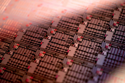
Imec and its partners in the GaN industrial affiliation program (IIAP) have produced device-quality wafers with GaN/AlGaN layers on 200mm silicon wafers. With these wafers, functional GaN MISHEMTs were processed using standard CMOS tools. The used processes are compatible with the strict contamination rules in a standard CMOS processing line (e.g. no use of gold). These first GaN devices on 200mm wafers are an important milestone on the path to cost-effective production of power devices in high-productivity 200mm fabs.
Imec processes first power devices on 200mm CMOS-compatible GaN-on-Si
Leuven, Belgium | Posted on May 26th, 2011GaN is a promising material for next-generation power devices with a performance beyond what is possible with silicon. Imec has recently succeeded in producing 200mm GaN-on-Si wafers with crack-free surfaces and a bow of less than 50�m. The wafers were made using an advanced MOCVD system from Applied Materials. The ability to use 200mm wafers is an important milestone, because it brings processing in reach of regular high-productivity 200mm fabs, allowing for an important cost reduction compared to processing smaller wafers on dedicated processing lines.
A second prerequisite for cost-effective processing, next to the wafer size, is that power devices can be fabricated with processes that are compatible with standard CMOS processes and tools. Imec proved this by processing its GaN-on-Si wafers using standard CMOS tools, yielding functional GaN MISHEMTs (metal-insulator-semiconductor HEMT). All equipment was verified for its capability to handle the wafers, and required only minimal adjustments in software and hardware. Conventionally, gold is used for ohmic contacts and gate structures in power devices, but it makes GaN processing incompatible with conventional CMOS processing. To overcome this, imec based the ohmic contact formation on an Au-free metallization system, and modified the Schottky gate to a gate dielectric based gold-free metal-insulator-semiconductor (MIS) structure. This introduction of the MISHEMT structure had the added advantage of reducing the high leakage current of conventional HEMTs.
####
About IMEC
Imec performs world-leading research in nanoelectronics. Imec leverages its scientific knowledge with the innovative power of its global partnerships in ICT, healthcare and energy. Imec delivers industry-relevant technology solutions. In a unique high-tech environment, its international top talent is committed to providing the building blocks for a better life in a sustainable society. Imec is headquartered in Leuven, Belgium, and has offices in Belgium, the Netherlands, Taiwan, US, China and Japan. Its staff of about 1,900 people includes more than 500 industrial residents and guest researchers. In 2010, imec's revenue (P&L) was 285 million euro. Further information on imec can be found at www.imec.be.
Imec is a registered trademark for the activities of IMEC International (a legal entity set up under Belgian law as a "stichting van openbaar nut�), imec Belgium (IMEC vzw supported by the Flemish Government), imec the Netherlands (Stichting IMEC Nederland, part of Holst Centre which is supported by the Dutch Government), imec Taiwan (IMEC Taiwan Co.) and imec China (IMEC Microelectronics (Shangai) Co. Ltd.).
For more information, please click here
Contacts:
Katrien Marent
Director of External Communications
T: +32 16 28 18 80
Mobile: +32 474 30 28 66
Copyright © IMEC
If you have a comment, please Contact us.Issuers of news releases, not 7th Wave, Inc. or Nanotechnology Now, are solely responsible for the accuracy of the content.
Bookmark:


| Related News Press |
News and information
![]() Simulating magnetization in a Heisenberg quantum spin chain April 5th, 2024
Simulating magnetization in a Heisenberg quantum spin chain April 5th, 2024
![]() NRL charters Navy�s quantum inertial navigation path to reduce drift April 5th, 2024
NRL charters Navy�s quantum inertial navigation path to reduce drift April 5th, 2024
![]() Discovery points path to flash-like memory for storing qubits: Rice find could hasten development of nonvolatile quantum memory April 5th, 2024
Discovery points path to flash-like memory for storing qubits: Rice find could hasten development of nonvolatile quantum memory April 5th, 2024
Chip Technology
![]() Discovery points path to flash-like memory for storing qubits: Rice find could hasten development of nonvolatile quantum memory April 5th, 2024
Discovery points path to flash-like memory for storing qubits: Rice find could hasten development of nonvolatile quantum memory April 5th, 2024
![]() Utilizing palladium for addressing contact issues of buried oxide thin film transistors April 5th, 2024
Utilizing palladium for addressing contact issues of buried oxide thin film transistors April 5th, 2024
![]() HKUST researchers develop new integration technique for efficient coupling of III-V and silicon February 16th, 2024
HKUST researchers develop new integration technique for efficient coupling of III-V and silicon February 16th, 2024
Announcements
![]() NRL charters Navy�s quantum inertial navigation path to reduce drift April 5th, 2024
NRL charters Navy�s quantum inertial navigation path to reduce drift April 5th, 2024
![]() Discovery points path to flash-like memory for storing qubits: Rice find could hasten development of nonvolatile quantum memory April 5th, 2024
Discovery points path to flash-like memory for storing qubits: Rice find could hasten development of nonvolatile quantum memory April 5th, 2024
Alliances/Trade associations/Partnerships/Distributorships
![]() Chicago Quantum Exchange welcomes six new partners highlighting quantum technology solutions, from Chicago and beyond September 23rd, 2022
Chicago Quantum Exchange welcomes six new partners highlighting quantum technology solutions, from Chicago and beyond September 23rd, 2022
![]() University of Illinois Chicago joins Brookhaven Lab's Quantum Center June 10th, 2022
University of Illinois Chicago joins Brookhaven Lab's Quantum Center June 10th, 2022
|
|
||
|
|
||
| The latest news from around the world, FREE | ||
|
|
||
|
|
||
| Premium Products | ||
|
|
||
|
Only the news you want to read!
Learn More |
||
|
|
||
|
Full-service, expert consulting
Learn More |
||
|
|
||