Home > Press > Boosting Memory Chips
 |
Abstract:
Moore's law predicts that the number of transistors on a silicon chip will double approximately every two years. Thanks to nano technology a similar acceleration is observed in data storage capability of memory chips
Boosting Memory Chips
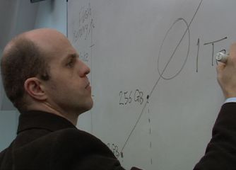
Italy | Posted on April 19th, 2011In each generation cycle memory chips get smaller and less expensive, but can hold more data. They are used in USB memory sticks, personal computers, video consoles and many other electronic devices. Further advances in electronics' technology rely now on the development of new materials and in particular on their manufacture in nano scale thin films. Atomic Layer Deposition (ALD) is a way to manufacture metal oxide materials layer by layer on the nano scale.
Within the EU research project REALISE synthetic chemists, materials scientists, electronic engineers and commercial project partners from all over Europe developed together an optimized process for nano scale deposition for the semiconductor manufacturing.
"Improvements in memory chips are now only possible by bringing in new materials that can be laid down with the high quality needed", says project coordinator Simon Elliott from Tyndall National Institute in Cork, Ireland.
The new materials are rare earth oxides: A fine powder that functions as an electronic insulator. It will isolate the electrical information on computer chips. The aim is to achieve a high dielectric material, with a so called high k-value, which would enable a large capacitance.
ASM Microchemistry in Helsinki, Finland, the chemical manufacturer partner in the project, has developed reactors that are able to deposit the rare earth oxides onto silicon wafers in a semi conductor line. The new process allows the scientists to put down these particular high-k dielectric films with a very high control and a very good quality and to do all that under clean room conditions.
Particle checks, electrical tests and measuring of the uniformity of the thickness have also been done with the processed wafers. The results are promising. All the elements are in place for the semi conductor industry to take on this new material when they are ready and produce the memory chip of the future.
####
For more information, please click here
Contacts:
Elisabeth Schmid
Phone: + 39 02 700 25 71
Fax: + 39 02 700 25 40
E-mail:
Copyright © youris.com
If you have a comment, please Contact us.Issuers of news releases, not 7th Wave, Inc. or Nanotechnology Now, are solely responsible for the accuracy of the content.
Bookmark:


| Related News Press |
News and information
![]() Simulating magnetization in a Heisenberg quantum spin chain April 5th, 2024
Simulating magnetization in a Heisenberg quantum spin chain April 5th, 2024
![]() NRL charters Navy�s quantum inertial navigation path to reduce drift April 5th, 2024
NRL charters Navy�s quantum inertial navigation path to reduce drift April 5th, 2024
![]() Discovery points path to flash-like memory for storing qubits: Rice find could hasten development of nonvolatile quantum memory April 5th, 2024
Discovery points path to flash-like memory for storing qubits: Rice find could hasten development of nonvolatile quantum memory April 5th, 2024
Chip Technology
![]() Discovery points path to flash-like memory for storing qubits: Rice find could hasten development of nonvolatile quantum memory April 5th, 2024
Discovery points path to flash-like memory for storing qubits: Rice find could hasten development of nonvolatile quantum memory April 5th, 2024
![]() Utilizing palladium for addressing contact issues of buried oxide thin film transistors April 5th, 2024
Utilizing palladium for addressing contact issues of buried oxide thin film transistors April 5th, 2024
![]() HKUST researchers develop new integration technique for efficient coupling of III-V and silicon February 16th, 2024
HKUST researchers develop new integration technique for efficient coupling of III-V and silicon February 16th, 2024
Memory Technology
![]() Utilizing palladium for addressing contact issues of buried oxide thin film transistors April 5th, 2024
Utilizing palladium for addressing contact issues of buried oxide thin film transistors April 5th, 2024
![]() Interdisciplinary: Rice team tackles the future of semiconductors Multiferroics could be the key to ultralow-energy computing October 6th, 2023
Interdisciplinary: Rice team tackles the future of semiconductors Multiferroics could be the key to ultralow-energy computing October 6th, 2023
![]() Researchers discover materials exhibiting huge magnetoresistance June 9th, 2023
Researchers discover materials exhibiting huge magnetoresistance June 9th, 2023
Announcements
![]() NRL charters Navy�s quantum inertial navigation path to reduce drift April 5th, 2024
NRL charters Navy�s quantum inertial navigation path to reduce drift April 5th, 2024
![]() Discovery points path to flash-like memory for storing qubits: Rice find could hasten development of nonvolatile quantum memory April 5th, 2024
Discovery points path to flash-like memory for storing qubits: Rice find could hasten development of nonvolatile quantum memory April 5th, 2024
Alliances/Trade associations/Partnerships/Distributorships
![]() Chicago Quantum Exchange welcomes six new partners highlighting quantum technology solutions, from Chicago and beyond September 23rd, 2022
Chicago Quantum Exchange welcomes six new partners highlighting quantum technology solutions, from Chicago and beyond September 23rd, 2022
![]() University of Illinois Chicago joins Brookhaven Lab's Quantum Center June 10th, 2022
University of Illinois Chicago joins Brookhaven Lab's Quantum Center June 10th, 2022
|
|
||
|
|
||
| The latest news from around the world, FREE | ||
|
|
||
|
|
||
| Premium Products | ||
|
|
||
|
Only the news you want to read!
Learn More |
||
|
|
||
|
Full-service, expert consulting
Learn More |
||
|
|
||