Home > Press > DirectOverlay display & analysis software from JPK Instruments
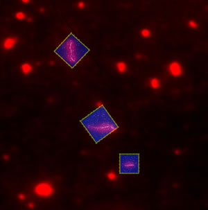 |
| An example of the power of DirectOverlay from JPK: A fluorescence image highlights three individual labelled DNA molecules while the 3D image zooms in to a high resolution 700nm AFM image. (Sample courtesy of Dr. M. Modesti, CNRS Marseilles) |
Abstract:
JPK Instruments, a world-leading manufacturer of nanoanalytic instrumentation for research in life sciences and soft matter, provides a unique software package to make the display of light microscopy images together with atomic force microscopy images a seamless exercise. This package is called DirectOverlay™.
DirectOverlay display & analysis software from JPK Instruments
Berlin, Germany | Posted on April 19th, 2011Atomic force microscopy (AFM) is a powerful tool to investigate a huge variety of different samples with nanometre scale resolution under physiological conditions. As well as providing topographic measurements, information about interaction forces and mechanical properties like adhesion and elasticity can also be obtained. Perfect integration of AFM with an optical setup can increase the range of applications and opens up many possibilities for correlating structural information with optical information such as functionalized labelling of certain components.
To achieve the perfect combination of optics and AFM at the molecular scale, distortions must be prevented. This will result in two images, such as optical and AFM images, that do not perfectly overlay. Reasons for distortions include aberrations arising from the lenses and mirrors of the optics system. This nonlinear stretching, rotating and offsetting of optical images are present in nearly all types of optical setups.
To generate a seamless overlay of both techniques, JPK developed a cutting-edge calibration method, called DirectOverlay, which uses the accuracy of the AFM closed-loop scanning system to enable a true display of absolute angles and length coordinates. The calibration procedure is done automatically and uses the known positions and offsets of the cantilever to calibrate the optical image into the AFM coordinates. To generate a perfect match of the optical and AFM image, 25 or more points are used in the calibration algorithm. At each point, an optical image is acquired and the position of the cantilever tip is automatically detected in each optical image without needing input on cantilever angle, shape or magnification. The algorithm then performs a nonlinear conversion and, as a result, the optical image is corrected for any lens imperfections and converted into the linearized AFM length coordinates. This provides a perfect integration of optical and AFM data with sub-diffraction limit precision.
Finally, the calibrated optical image is transferred into the JPK SPM software, so that AFM scan regions can be selected within the optical image. Direct "in optical image" selection of AFM measurements (imaging, mapping and force spectroscopy) leads to more efficient experiments and reduces dramatically overview image scanning in AFM.
JPK develop, engineer and manufacture instrumentation in Germany to the world-recognized standards of German precision engineering, quality and functionality. For further details on the NanoWizard® 3 systems and other products in the JPK family of nanoscale characterization systems, please contact JPK on +49 30533112070 or visit the JPK web site, (www.jpk.com/nanowizard-3-directoverlay-tm.538.en.html).
####
About JPK Instruments (JPK)
JPK Instruments AG is a world-leading manufacturer of nanoanalytic instruments - particularly atomic force microscope (AFM) systems and optical tweezers - for a broad range of applications reaching from soft matter physics to nano-optics, from surface chemistry to cell and molecular biology. From its earliest days applying atomic force microscope (AFM) technology, JPK has recognized the opportunities provided by nanotechnology for transforming life sciences and soft matter research. This focus has driven JPK’s success in uniting the worlds of nanotechnology tools and life science applications by offering cutting-edge technology and unique applications expertise. Headquartered in Berlin and with direct operations in Dresden, Cambridge (UK), Singapore, Tokyo (Japan) and Paris (France), JPK maintains a global network of distributors and support centers and provides on the spot applications and service support to an ever-growing community of researchers.
For more information, please click here
Contacts:
+49 (0) 30 5331 12070
For further information
please contact either:
Jezz Leckenby
NetDyaLog Limited
T: +44 (0) 1799 521881
M: +44 (0) 7843 012997
or
Claudia Boettcher
JPK Instruments
T: +49 (0) 30 5331 12070
Copyright © JPK Instruments (JPK)
If you have a comment, please Contact us.Issuers of news releases, not 7th Wave, Inc. or Nanotechnology Now, are solely responsible for the accuracy of the content.
Bookmark:


| Related News Press |
News and information
![]() Simulating magnetization in a Heisenberg quantum spin chain April 5th, 2024
Simulating magnetization in a Heisenberg quantum spin chain April 5th, 2024
![]() NRL charters Navy’s quantum inertial navigation path to reduce drift April 5th, 2024
NRL charters Navy’s quantum inertial navigation path to reduce drift April 5th, 2024
![]() Discovery points path to flash-like memory for storing qubits: Rice find could hasten development of nonvolatile quantum memory April 5th, 2024
Discovery points path to flash-like memory for storing qubits: Rice find could hasten development of nonvolatile quantum memory April 5th, 2024
Imaging
![]() Nanoscale CL thermometry with lanthanide-doped heavy-metal oxide in TEM March 8th, 2024
Nanoscale CL thermometry with lanthanide-doped heavy-metal oxide in TEM March 8th, 2024
![]() The USTC realizes In situ electron paramagnetic resonance spectroscopy using single nanodiamond sensors November 3rd, 2023
The USTC realizes In situ electron paramagnetic resonance spectroscopy using single nanodiamond sensors November 3rd, 2023
![]() Observation of left and right at nanoscale with optical force October 6th, 2023
Observation of left and right at nanoscale with optical force October 6th, 2023
Software
![]() Visualizing nanoscale structures in real time: Open-source software enables researchers to see materials in 3D while they're still on the electron microscope August 19th, 2022
Visualizing nanoscale structures in real time: Open-source software enables researchers to see materials in 3D while they're still on the electron microscope August 19th, 2022
![]() Luisier wins SNSF Advanced Grant to develop simulation tools for nanoscale devices July 8th, 2022
Luisier wins SNSF Advanced Grant to develop simulation tools for nanoscale devices July 8th, 2022
![]() Oxford Instruments’ Atomfab® system is production-qualified at a market-leading GaN power electronics device manufacturer December 17th, 2021
Oxford Instruments’ Atomfab® system is production-qualified at a market-leading GaN power electronics device manufacturer December 17th, 2021
Announcements
![]() NRL charters Navy’s quantum inertial navigation path to reduce drift April 5th, 2024
NRL charters Navy’s quantum inertial navigation path to reduce drift April 5th, 2024
![]() Discovery points path to flash-like memory for storing qubits: Rice find could hasten development of nonvolatile quantum memory April 5th, 2024
Discovery points path to flash-like memory for storing qubits: Rice find could hasten development of nonvolatile quantum memory April 5th, 2024
Tools
![]() Ferroelectrically modulate the Fermi level of graphene oxide to enhance SERS response November 3rd, 2023
Ferroelectrically modulate the Fermi level of graphene oxide to enhance SERS response November 3rd, 2023
![]() The USTC realizes In situ electron paramagnetic resonance spectroscopy using single nanodiamond sensors November 3rd, 2023
The USTC realizes In situ electron paramagnetic resonance spectroscopy using single nanodiamond sensors November 3rd, 2023
|
|
||
|
|
||
| The latest news from around the world, FREE | ||
|
|
||
|
|
||
| Premium Products | ||
|
|
||
|
Only the news you want to read!
Learn More |
||
|
|
||
|
Full-service, expert consulting
Learn More |
||
|
|
||