Home > Press > NT-MDT Co. opens a new R&D office in the USA
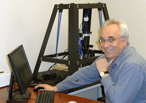 |
| Dr. Sergei Magonov |
Abstract:
NT-MDT Development in Tempe, Arizona, is a new team of NT-MDT Co. The experienced AFM developers Sergei Magonov, John Alexander and Sergey Belikov have joined the company.
NT-MDT Co. opens a new R&D office in the USA
Tempe, AZ | Posted on April 19th, 2011To address the increasing activity of NT-MDT Co. on the US and world markets of scanning probe microscopy equipment, the company has invited the experienced AFM developers and practitioners: Sergei Magonov, John Alexander and Sergey Belikov to form the research unit NT-MDT Development in Tempe, Arizona.
This team, which has combined SPM experience of almost 60 years, will focus its efforts on developments and applications of novel multi-frequency SPM techniques related to quantitative nanomechanical and electric measurements of various materials
The leader of the team Dr. Sergei Magonov was educated in the former USSR where he got his PhD and has conducted research on polymers in the Russian Academy of Sciences.
In 1988 Dr. Magonov moved to Germany (Freiburg University) where he applied the first scanning tunneling microscopy (STM) and the atomic force microscopy (AFM) to different materials. The scientific results obtained in this period were summarized in the book (written jointly with Prof. M. Whangbo) "Surface Analysis with STM and AFM", VCH Weinheim 1996.
In 1995 Sergei joined Digital Instruments - a manufacturer of the scanning probe microscopes where he was involved in development of various AFM applications to soft materials. After spending 12 years with Digital Instruments/Veeco Instruments he moved in 2007 to Agilent Technologies, another manufacturer of scanning probe microscopy, where he continued the research in AFM.
John Alexander became familiar with SPM in 1986 when he was designing a low-temperature STM microscope during his physics studies in Akron University. After graduation with Masters in Physics in 1988 John entered one of the first SPM businesses - Angstrom Technology Inc. in Arizona.
For the 20 plus years John Alexander has worked as the leading electronics and system engineer in several companies manufacturing scanning probe microscopes: Park Scientific, KLM-Tencor, Molecular Imaging, and most recently at Agilent Technologies.
He is coauthor of a number research articles and 6 US patents in scanning probe microscopy. Recent interests are in the development of multi frequency AFM measurements.
Sergey Belikov educated in former USSR where he received MS at Kiev Polytechnic Institute and PhD at Institute of Cybernetics of Ukrainian Academy of Sciences. His research activities in mathematics were focused on developments of averaging methods recently applied in AFM.
Since 1991 Sergey is working in a number of research institutions and companies in the USA where his expertise was implemented in development of different software for various research and industrial control applications.
Dr. Belikov's activities in scanning probe microscopy were established during his employment at Veeco Instruments (2001-2008) where he played the key role in design of nanomechanical analysis package and other applications. Before joining the NT-MDT Development Sergey worked in 3M Company. Sergey is a coauthor of 10 patents and over 70 research papers.
The NT-MDT Development started the activities in April 2011.
####
About NT-MDT
Our mission is to enable researchers, engineers and developers to conduct nanoscale research by creating ever more perfect nanotechnology instrumentation. Along the way, we maintain a global perspective, always taking into consideration the needs of student in the classroom, the researcher at the cutting edge in the laboratory, and the practicalities of industrial R&D.
For more information, please click here
Contacts:
Natalia Karagicheva
PR Manager of Marketing Dept.
Phone: +7 (495) 913-57-36/37/38
Fax: +7 (495) 913-57-39
E-mail:
Copyright © NT-MDT
If you have a comment, please Contact us.Issuers of news releases, not 7th Wave, Inc. or Nanotechnology Now, are solely responsible for the accuracy of the content.
Bookmark:


| Related News Press |
News and information
![]() Simulating magnetization in a Heisenberg quantum spin chain April 5th, 2024
Simulating magnetization in a Heisenberg quantum spin chain April 5th, 2024
![]() NRL charters Navy�s quantum inertial navigation path to reduce drift April 5th, 2024
NRL charters Navy�s quantum inertial navigation path to reduce drift April 5th, 2024
![]() Discovery points path to flash-like memory for storing qubits: Rice find could hasten development of nonvolatile quantum memory April 5th, 2024
Discovery points path to flash-like memory for storing qubits: Rice find could hasten development of nonvolatile quantum memory April 5th, 2024
Imaging
![]() Nanoscale CL thermometry with lanthanide-doped heavy-metal oxide in TEM March 8th, 2024
Nanoscale CL thermometry with lanthanide-doped heavy-metal oxide in TEM March 8th, 2024
![]() The USTC realizes In situ electron paramagnetic resonance spectroscopy using single nanodiamond sensors November 3rd, 2023
The USTC realizes In situ electron paramagnetic resonance spectroscopy using single nanodiamond sensors November 3rd, 2023
![]() Observation of left and right at nanoscale with optical force October 6th, 2023
Observation of left and right at nanoscale with optical force October 6th, 2023
Openings/New facilities/Groundbreaking/Expansion
![]() OCSiAl expands its graphene nanotube production capacities to Europe June 17th, 2022
OCSiAl expands its graphene nanotube production capacities to Europe June 17th, 2022
![]() GLOBALFOUNDRIES Moves Corporate Headquarters to its Most Advanced Semiconductor Manufacturing Facility in New York April 27th, 2021
GLOBALFOUNDRIES Moves Corporate Headquarters to its Most Advanced Semiconductor Manufacturing Facility in New York April 27th, 2021
![]() Oxford Instruments Plasma Technology relocates to advanced manufacturing facility: Move driven by exceptional business growth February 12th, 2021
Oxford Instruments Plasma Technology relocates to advanced manufacturing facility: Move driven by exceptional business growth February 12th, 2021
Announcements
![]() NRL charters Navy�s quantum inertial navigation path to reduce drift April 5th, 2024
NRL charters Navy�s quantum inertial navigation path to reduce drift April 5th, 2024
![]() Discovery points path to flash-like memory for storing qubits: Rice find could hasten development of nonvolatile quantum memory April 5th, 2024
Discovery points path to flash-like memory for storing qubits: Rice find could hasten development of nonvolatile quantum memory April 5th, 2024
Tools
![]() Ferroelectrically modulate the Fermi level of graphene oxide to enhance SERS response November 3rd, 2023
Ferroelectrically modulate the Fermi level of graphene oxide to enhance SERS response November 3rd, 2023
![]() The USTC realizes In situ electron paramagnetic resonance spectroscopy using single nanodiamond sensors November 3rd, 2023
The USTC realizes In situ electron paramagnetic resonance spectroscopy using single nanodiamond sensors November 3rd, 2023
Patents/IP/Tech Transfer/Licensing
![]() Getting drugs across the blood-brain barrier using nanoparticles March 3rd, 2023
Getting drugs across the blood-brain barrier using nanoparticles March 3rd, 2023
![]() Metasurfaces control polarized light at will: New research unlocks the hidden potential of metasurfaces August 13th, 2021
Metasurfaces control polarized light at will: New research unlocks the hidden potential of metasurfaces August 13th, 2021
![]() Arrowhead Pharmaceuticals Announces Closing of Agreement with Takeda November 27th, 2020
Arrowhead Pharmaceuticals Announces Closing of Agreement with Takeda November 27th, 2020
|
|
||
|
|
||
| The latest news from around the world, FREE | ||
|
|
||
|
|
||
| Premium Products | ||
|
|
||
|
Only the news you want to read!
Learn More |
||
|
|
||
|
Full-service, expert consulting
Learn More |
||
|
|
||