Home > Press > Getting the Point: Real-Time Monitoring of Atomic-Microscope Probes Adjusts for Wear
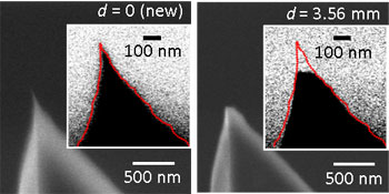 |
| As an atomic force microscope�s tip degrades, the change in tip size and shape affects its resonant frequency and that can be used to accurately measure, in real time, the change in the tip�s shape, thereby resulting in more accurate measurements and images at nanometer size scales. Credit: Jason Killgore, NIST |
Abstract:
Scientists at the National Institute of Standards and Technology (NIST) have developed a way to measure the wear and degradation of the microscopic probes used to study nanoscale structures in situ and as it's happening. Their technique can both dramatically speed up and improve the accuracy of the most precise and delicate nanoscale measurements done with atomic force microscopy (AFM).
Getting the Point: Real-Time Monitoring of Atomic-Microscope Probes Adjusts for Wear
Gaithersburg, MD | Posted on March 31st, 2011If you're trying to measure the contours of a surface with a ruler that's crumbling away as you work, then you at least need to know how fast and to what extent it is being worn away during the measurement.
This has been the challenge for researchers and manufacturers trying to create images of the surfaces of nanomaterials and nanostructures. Taking a photo is impossible at such small scales, so researchers use atomic force microscopes. Think of a device like a phonograph needle being used, on a nanoscale, to measure the peaks and valleys as it's dragged back and forth across a surface. These devices are used extensively in nanoscale imaging to measure the contours of nanostructures, but the AFM tips are so small that they tend to wear down as they traverse the surface being measured.
Today, most researchers stop the measurement to "take a picture" of the tip with an electron microscope, a time-consuming method prone to inaccuracies.
NIST materials engineer Jason Killgore has developed a method for measuring in real time the extent to which AFM tips wear down. Killgore measures the resonant frequency of the AFM sensor tip, a natural vibration rate like that of a tuning fork, while the instrument is in use. Because changes to the size and shape of the tip affect its resonant frequency, he is able to measure the size of the AFM's tip as it works�in increments of a tenth of a nanometer, essentially atomic scale resolution. The technique, called contact resonance force microscopy, is described in a paper recently published in the journal Small.*
The potential impact of this development is considerable. Thousands of AFMs are in use at universities, manufacturing plants and research and development facilities around the world. Improving their ability to measure and image nanosized devices will improve the quality and effectiveness of those devices. Another benefit is that developing new measurement tips�and studying the properties of new materials used in those tips�will be much easier and faster, given the immediate feedback about wear rates.
* J. P. Killgore, R. H. Geiss and D. C. Hurley. Continuous measurement of AFM tip wear by contact resonance force microscopy. Small. Published March 15, 2011.
####
For more information, please click here
Contacts:
James Burrus
303-497-4789
Copyright © NIST
If you have a comment, please Contact us.Issuers of news releases, not 7th Wave, Inc. or Nanotechnology Now, are solely responsible for the accuracy of the content.
Bookmark:


| Related News Press |
News and information
![]() Simulating magnetization in a Heisenberg quantum spin chain April 5th, 2024
Simulating magnetization in a Heisenberg quantum spin chain April 5th, 2024
![]() NRL charters Navy�s quantum inertial navigation path to reduce drift April 5th, 2024
NRL charters Navy�s quantum inertial navigation path to reduce drift April 5th, 2024
![]() Discovery points path to flash-like memory for storing qubits: Rice find could hasten development of nonvolatile quantum memory April 5th, 2024
Discovery points path to flash-like memory for storing qubits: Rice find could hasten development of nonvolatile quantum memory April 5th, 2024
Imaging
![]() Nanoscale CL thermometry with lanthanide-doped heavy-metal oxide in TEM March 8th, 2024
Nanoscale CL thermometry with lanthanide-doped heavy-metal oxide in TEM March 8th, 2024
![]() The USTC realizes In situ electron paramagnetic resonance spectroscopy using single nanodiamond sensors November 3rd, 2023
The USTC realizes In situ electron paramagnetic resonance spectroscopy using single nanodiamond sensors November 3rd, 2023
![]() Observation of left and right at nanoscale with optical force October 6th, 2023
Observation of left and right at nanoscale with optical force October 6th, 2023
Discoveries
![]() Chemical reactions can scramble quantum information as well as black holes April 5th, 2024
Chemical reactions can scramble quantum information as well as black holes April 5th, 2024
![]() New micromaterial releases nanoparticles that selectively destroy cancer cells April 5th, 2024
New micromaterial releases nanoparticles that selectively destroy cancer cells April 5th, 2024
![]() Utilizing palladium for addressing contact issues of buried oxide thin film transistors April 5th, 2024
Utilizing palladium for addressing contact issues of buried oxide thin film transistors April 5th, 2024
Announcements
![]() NRL charters Navy�s quantum inertial navigation path to reduce drift April 5th, 2024
NRL charters Navy�s quantum inertial navigation path to reduce drift April 5th, 2024
![]() Discovery points path to flash-like memory for storing qubits: Rice find could hasten development of nonvolatile quantum memory April 5th, 2024
Discovery points path to flash-like memory for storing qubits: Rice find could hasten development of nonvolatile quantum memory April 5th, 2024
Tools
![]() Ferroelectrically modulate the Fermi level of graphene oxide to enhance SERS response November 3rd, 2023
Ferroelectrically modulate the Fermi level of graphene oxide to enhance SERS response November 3rd, 2023
![]() The USTC realizes In situ electron paramagnetic resonance spectroscopy using single nanodiamond sensors November 3rd, 2023
The USTC realizes In situ electron paramagnetic resonance spectroscopy using single nanodiamond sensors November 3rd, 2023
|
|
||
|
|
||
| The latest news from around the world, FREE | ||
|
|
||
|
|
||
| Premium Products | ||
|
|
||
|
Only the news you want to read!
Learn More |
||
|
|
||
|
Full-service, expert consulting
Learn More |
||
|
|
||