Home > Press > Atomic switches: Ionic computing
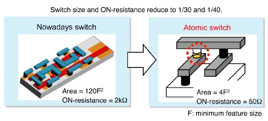 |
| Figure 1: Comparison between semiconductor-transistor-based and atomic-switch-based switching circuits. |
Abstract:
A critical review of the current status and future prospects of new computing architectures based on ‘atomic switches' fabricated by controlling the movement of cationic ions during solid electrochemical reactions.
Atomic switches: Ionic computing
Japan | Posted on March 24th, 2011A review of new types of nanodevices and computing based on cationic-based atomic switches is presented Takami Hino and coworkers at the WPI Center for Materials Nanoarchitectonics at the National Institute for Materials Science (NIMS) in Tsukuba, Japan. The review paper is published this month in the journal Science and Technology of Advanced Materials.
The researchers describe the fundamental mechanisms governing the operation of nanoionic atomic switches with detailed examples of their own three terminal devices, and predict a bright future for integrating atomic switches with conventional silicon devices by using ionic conductive materials.
Mechanical atomic switches—operated by manipulating atoms between a conducting surface and the tip of a scanning tunneling microscope (STM)—were first reported in the early 1990s. These mechanical switches triggered intense interest in the development of electrically controlled atomic switches, produced by the movement of cationic ions in solid electrochemical reactions, where the operation of cationic atomic switches is governed by the formation of a conducting channel either in or on an ionic conductor.
Now, the challenge for researchers in this field is the fabrication of nanoionic device structures that can be integrated with conventional metal oxide silicon semiconductor devices.
In its simplest configuration, the operation of a nanoionic atomic switch consists of the formation and disintegration of nanometer sized metallic wires via a solid electrochemical reaction, which leads to major changes in the resistance between electrodes—the ‘on' and ‘off' states.
In this review, Hino and colleagues describe the control of silver ions in silver sulphide—an ionic conductor— using an STM tip to inject electrons to produce silver protrusions on the surface of silver sulphide, and their shrinkage by applying an appropriate bias voltage between the STM tip and electrode. Importantly, the application of a positive bias between a silver sulphide tip and a platinum surface leads to the growth of silver wires and a negative bias led their shrinkage. This bipolar control is important for practical device applications.
Gap-type atomic switches are a fundamental building block for bipolar nanoionic devices. Here, the researchers give a detailed account of bipolar switching using silver sulphide STM tips and platinum electrodes based on their own experiments on ‘crossbar' device structures with a 1 nm gap between silver sulphide and platinum, with emphasis on the physical mechanism governing high speed switching at 1 MHz, and the finding that switching time decreases exponentially with increasing bias voltage. The authors stress that the development of a reproducible method for fabricating ‘crossbar' devices was a major breakthrough, which enabled the first demonstration of nanoionic circuits such as logic gates.
With a view to practical applications of atomic switches, the authors give examples of advanced atomic switches including gapless-type devices consisting of metal/ionic conductor/metal structures, where one of the metals is electrochemically active and the other inert. Notably, recent reports on the use of metal oxides as ionic conductors have added further momentum for device commercialization.
Notably, gapless atomic switches also act as so-called ‘memristors' (memory resistors)—passive two terminal multi-state memory devices—where the size of the nanowire protrusion governs the operation characteristics.
Other advanced atomic switches include: three terminal devices such as structures with a solid copper sulphide electrolyte, where the formation of a copper bridge between a platinum-source electrode and copper-drain electrode is controlled by a copper gate-electrode; and photoassisted atomic switches, which do not require nanogaps, and nanowire protrusions are grown by optical irradiation of a photoconductive material located between the anion and electron conducting electrode and a counter metal electrode. Intriguingly, since the switch is turned ‘on' when the growing metal protrusion reaches the counter electrode, and the protrusion does not grow in the dark, the photoassisted atomic switch behaves as a programmable switch that could be used in erasable programmable read-only memory (EPROM).
The authors also describe the ‘learning abilities' of atomic switches capable of short-term and long-term memories in single nanoionic devices; nonvolatile bipolar switches; two terminal atomic switch logic gates; and field programmable gate arrays integrated with CMOS devices.
This review contains 77 references and 20 figures and provides an invaluable source of up-to-date information for newcomers and experts in this exciting area of research.
####
Contacts:
National Institute for Materials Science
Tsukuba, Japan
Email:
Tel. +81-(0)29-859-2494
Copyright © National Institute for Materials Science
If you have a comment, please Contact us.Issuers of news releases, not 7th Wave, Inc. or Nanotechnology Now, are solely responsible for the accuracy of the content.
Bookmark:


| Related Links |
![]() [2] National Institute for Materials Science:
[2] National Institute for Materials Science:
![]() [3] The International Center for Materials Nanoarchitectonics (MANA)
[3] The International Center for Materials Nanoarchitectonics (MANA)
| Related News Press |
News and information
![]() Simulating magnetization in a Heisenberg quantum spin chain April 5th, 2024
Simulating magnetization in a Heisenberg quantum spin chain April 5th, 2024
![]() NRL charters Navy’s quantum inertial navigation path to reduce drift April 5th, 2024
NRL charters Navy’s quantum inertial navigation path to reduce drift April 5th, 2024
![]() Discovery points path to flash-like memory for storing qubits: Rice find could hasten development of nonvolatile quantum memory April 5th, 2024
Discovery points path to flash-like memory for storing qubits: Rice find could hasten development of nonvolatile quantum memory April 5th, 2024
Imaging
![]() Nanoscale CL thermometry with lanthanide-doped heavy-metal oxide in TEM March 8th, 2024
Nanoscale CL thermometry with lanthanide-doped heavy-metal oxide in TEM March 8th, 2024
![]() The USTC realizes In situ electron paramagnetic resonance spectroscopy using single nanodiamond sensors November 3rd, 2023
The USTC realizes In situ electron paramagnetic resonance spectroscopy using single nanodiamond sensors November 3rd, 2023
![]() Observation of left and right at nanoscale with optical force October 6th, 2023
Observation of left and right at nanoscale with optical force October 6th, 2023
Molecular Machines
![]() First electric nanomotor made from DNA material: Synthetic rotary motors at the nanoscale perform mechanical work July 22nd, 2022
First electric nanomotor made from DNA material: Synthetic rotary motors at the nanoscale perform mechanical work July 22nd, 2022
![]() Nanotech scientists create world's smallest origami bird March 17th, 2021
Nanotech scientists create world's smallest origami bird March 17th, 2021
![]() Giant nanomachine aids the immune system: Theoretical chemistry August 28th, 2020
Giant nanomachine aids the immune system: Theoretical chemistry August 28th, 2020
Chip Technology
![]() Discovery points path to flash-like memory for storing qubits: Rice find could hasten development of nonvolatile quantum memory April 5th, 2024
Discovery points path to flash-like memory for storing qubits: Rice find could hasten development of nonvolatile quantum memory April 5th, 2024
![]() Utilizing palladium for addressing contact issues of buried oxide thin film transistors April 5th, 2024
Utilizing palladium for addressing contact issues of buried oxide thin film transistors April 5th, 2024
![]() HKUST researchers develop new integration technique for efficient coupling of III-V and silicon February 16th, 2024
HKUST researchers develop new integration technique for efficient coupling of III-V and silicon February 16th, 2024
Nanoelectronics
![]() Interdisciplinary: Rice team tackles the future of semiconductors Multiferroics could be the key to ultralow-energy computing October 6th, 2023
Interdisciplinary: Rice team tackles the future of semiconductors Multiferroics could be the key to ultralow-energy computing October 6th, 2023
![]() Key element for a scalable quantum computer: Physicists from Forschungszentrum Jülich and RWTH Aachen University demonstrate electron transport on a quantum chip September 23rd, 2022
Key element for a scalable quantum computer: Physicists from Forschungszentrum Jülich and RWTH Aachen University demonstrate electron transport on a quantum chip September 23rd, 2022
![]() Reduced power consumption in semiconductor devices September 23rd, 2022
Reduced power consumption in semiconductor devices September 23rd, 2022
![]() Atomic level deposition to extend Moore’s law and beyond July 15th, 2022
Atomic level deposition to extend Moore’s law and beyond July 15th, 2022
Announcements
![]() NRL charters Navy’s quantum inertial navigation path to reduce drift April 5th, 2024
NRL charters Navy’s quantum inertial navigation path to reduce drift April 5th, 2024
![]() Discovery points path to flash-like memory for storing qubits: Rice find could hasten development of nonvolatile quantum memory April 5th, 2024
Discovery points path to flash-like memory for storing qubits: Rice find could hasten development of nonvolatile quantum memory April 5th, 2024
Tools
![]() Ferroelectrically modulate the Fermi level of graphene oxide to enhance SERS response November 3rd, 2023
Ferroelectrically modulate the Fermi level of graphene oxide to enhance SERS response November 3rd, 2023
![]() The USTC realizes In situ electron paramagnetic resonance spectroscopy using single nanodiamond sensors November 3rd, 2023
The USTC realizes In situ electron paramagnetic resonance spectroscopy using single nanodiamond sensors November 3rd, 2023
|
|
||
|
|
||
| The latest news from around the world, FREE | ||
|
|
||
|
|
||
| Premium Products | ||
|
|
||
|
Only the news you want to read!
Learn More |
||
|
|
||
|
Full-service, expert consulting
Learn More |
||
|
|
||