Home > Press > Asylum Research Introduces Electrochemical Strain Microscopy for Energy Storage Research
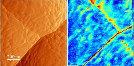 |
| The topographic image (left) of amorphous Si anode in the Si/LiPON/LiCoO2 thin-film battery structure shows the presence of a number of grain boundaries, as well as extensive surface roughness. The ESM image (right) is obtained by measuring the electrochemical strain hysteresis loops at each pixel (100x100 pixel image over 1 micron area). The area hysteresis loop is a measure of Li-ion mobility, and is plotted as 2D map (dark blue corresponds to closed loops, red to open loops). The enhanced Li-ion mobility along the sharp grain boundary is clearly seen, as well as localized hot spots on the diffuse grain boundary and within the grains. The effective resolution of ESM for this material is ~ 10 nm, providing a high-resolution view of Li-ion dynamics in these materials. (Reprinted from N. Balke, et al., Nano Lett. 10, 3420 (2010). |
Abstract:
Asylum Research, the technology leader in Scanning Probe and Atomic Force Microscopy (SPM/AFM), has announced the new Electrochemical Strain Microscopy (ESM) imaging technique for its Cypher™ and MFP-3D™ AFMs. Developed by Oak Ridge National Laboratory (ORNL) and Asylum Research, ESM is an innovative scanning probe microscopy (SPM) technique capable of probing electrochemical reactivity and ionic flows in solids on the sub-ten-nanometer level. ESM is the first technique that measures ionic currents directly, providing a new tool for mapping electrochemical phenomena on the nanoscale. The capability to probe electrochemical processes and ionic transport in solids is invaluable for a broad range of applications for energy generation and storage ranging from batteries to fuel cells. ESM has the potential to aid in these advances with two major improvements over other conventional technologies: (a) the resolution to probe nanometer-scale volumes and (b) the inherent ability to decouple ionic from electronic currents with (c) imaging capability extended to a broad range of spectroscopy techniques reminiscent of conventional electrochemical tools. Nina Balke of ORNL will be presenting recent results at the International Workshop on Scanning Probe Microscopy for Energy Applications (www.mpip-mainz.mpg.de/symposium/spm2011/) in Mainz, Germany, June 8-10 2011.
Asylum Research Introduces Electrochemical Strain Microscopy for Energy Storage Research
Santa Barbara, CA | Posted on March 15th, 2011Commented Roger Proksch, President of Asylum Research, "Progress in energy storage and conversion will be greatly facilitated by the ability to study batteries and fuel cells at the level of several nanometers. ESM provides functional imaging of electrochemical phenomena in volumes millions to a billion times smaller than conventional current-based electrochemical techniques. This new technique opens the pathway to understanding energy technology and ionic devices on the level of individual grains and defects, thus bridging macroscopic functionalities and atomistic mechanisms. This in turn will lead to improved energy storage solutions - batteries with extremely high energy densities and long lifetimes and fuel cells with very high energy densities and efficiencies."
"Traditionally, scanning probe microscopy techniques allowed measurement of electronic currents and short- and long-range forces," added Sergei Kalinin, Senior Research Staff Member in the Center for Nanophase Materials Sciences at ORNL and co-inventor (with Nina Balke and Stephen Jesse) of ESM. "ESM extends this capability to measure ionic currents, and has already been demonstrated for a variety of Li-ion cathode, anode, and electrolyte materials, as well as oxygen electrolytes and mixed electronic-ionic conductors. The ubiquitous presence of concentration-molar volume coupling in electrochemical systems suggests that this technique is in fact universal for solid state ionic imaging - from batteries and solid state to memristive electronics.
Stephen Jesse added "Perhaps even more importantly, the use of band excitation and DART engines allows measurements to be performed on rough surfaces of realistic electrochemical materials, making ESM useful for real materials and devices."
####
About Asylum Research
Asylum Research is the technology leader in atomic force and scanning probe microscopy (AFM/SPM) for both materials and bioscience applications. Founded in 1999, we are an employee owned company dedicated to innovative instrumentation for nanoscience and nanotechnology, with over 250 years combined AFM/SPM experience among our staff. Our instruments are used for a variety of nanoscience applications in material science, physics, polymers, chemistry, biomaterials, and bioscience, including single molecule mechanical experiments on DNA, protein unfolding and polymer elasticity, as well as force measurements for biomaterials, chemical sensing, polymers, colloidal forces, adhesion, and more. Asylum’s product line offers imaging and measurement capabilities for a wide range of samples, including advanced techniques such as electrical characterization (CAFM, KFM, EFM), high voltage piezoresponse force microscopy (PFM), thermal analysis, quantitative nanoindenting, and a wide range of environmental accessories and application-ready modules.
Asylum’s MFP-3D set the standard for AFM technology, with unprecedented precision and flexibility. The MFP-3D is the first AFM with true independent piezo positioning in all three axes, combined with low noise closed-loop feedback sensor technology. The MFP-3D offers both top and bottom sample viewing and easy integration with most commercially-available inverted optical microscopes.
Asylum’s new Cypher AFM is the world’s first new small sample AFM/SPM in over a decade, and sets the new standard as the world’s highest resolution AFM. Cypher provides low-drift closed loop atomic resolution for the most accurate images and measurements possible today, >20X faster AC imaging with small cantilevers, Spot-On™ automated laser and photodetector alignment for easy setup, integrated thermal, acoustic and vibration control, and broad support for all major AFM/SPM scanning modes and capabilities.
Asylum Research offers the lowest cost of ownership of any AFM company. Ask us about our industry-best 2-year warranty, our legendary product and applications support, and our exclusive 6-month money-back satisfaction guarantee. We are dedicated to providing the most technically advanced AFMs for researchers who want to take their experiments to the next level. Asylum Research also distributes third party cantilevers from Olympus, Nanoworld/Nanosensors, and our own MFM and iDrive™ tips.
About Oak Ridge National Laboratory
Oak Ridge National Laboratory is the Department of Energy's largest science and energy laboratory. ORNL has a staff of more than 4,800 and annually hosts approximately 3,000 guest researchers who spend two weeks or longer in Oak Ridge. As an international leader in a range of scientific areas that support the Department of Energy's mission, ORNL has six major mission roles: neutron science, energy, high-performance computing, systems biology, materials science at the nanoscale, and national security. ORNL's leadership role in the nation's energy future includes hosting the Center for Nanophase Materials Sciences - one of the five Department of Energy Nanoscale Science Research Centers, which serve as user facilities for interdisciplinary research at the nanoscale supported by the DOE Office of Science.
For more information, please click here
Contacts:
Jennifer Jones
Asylum Research Corp.
940 Main Campus Drive, Suite 130
Raleigh, NC 27606
919-828-6490 office*
919-828-6492 fax*
*new phone numbers
Corporate Office:
6310 Hollister Ave
Santa Barbara, CA 93117
805-696-6466 office
888-472-2795 toll free
Copyright © Asylum Research
If you have a comment, please Contact us.Issuers of news releases, not 7th Wave, Inc. or Nanotechnology Now, are solely responsible for the accuracy of the content.
Bookmark:


| Related News Press |
News and information
![]() Simulating magnetization in a Heisenberg quantum spin chain April 5th, 2024
Simulating magnetization in a Heisenberg quantum spin chain April 5th, 2024
![]() NRL charters Navy’s quantum inertial navigation path to reduce drift April 5th, 2024
NRL charters Navy’s quantum inertial navigation path to reduce drift April 5th, 2024
![]() Discovery points path to flash-like memory for storing qubits: Rice find could hasten development of nonvolatile quantum memory April 5th, 2024
Discovery points path to flash-like memory for storing qubits: Rice find could hasten development of nonvolatile quantum memory April 5th, 2024
Imaging
![]() Nanoscale CL thermometry with lanthanide-doped heavy-metal oxide in TEM March 8th, 2024
Nanoscale CL thermometry with lanthanide-doped heavy-metal oxide in TEM March 8th, 2024
Laboratories
![]() A battery’s hopping ions remember where they’ve been: Seen in atomic detail, the seemingly smooth flow of ions through a battery’s electrolyte is surprisingly complicated February 16th, 2024
A battery’s hopping ions remember where they’ve been: Seen in atomic detail, the seemingly smooth flow of ions through a battery’s electrolyte is surprisingly complicated February 16th, 2024
![]() NRL discovers two-dimensional waveguides February 16th, 2024
NRL discovers two-dimensional waveguides February 16th, 2024
Announcements
![]() NRL charters Navy’s quantum inertial navigation path to reduce drift April 5th, 2024
NRL charters Navy’s quantum inertial navigation path to reduce drift April 5th, 2024
![]() Discovery points path to flash-like memory for storing qubits: Rice find could hasten development of nonvolatile quantum memory April 5th, 2024
Discovery points path to flash-like memory for storing qubits: Rice find could hasten development of nonvolatile quantum memory April 5th, 2024
Tools
![]() Ferroelectrically modulate the Fermi level of graphene oxide to enhance SERS response November 3rd, 2023
Ferroelectrically modulate the Fermi level of graphene oxide to enhance SERS response November 3rd, 2023
![]() The USTC realizes In situ electron paramagnetic resonance spectroscopy using single nanodiamond sensors November 3rd, 2023
The USTC realizes In situ electron paramagnetic resonance spectroscopy using single nanodiamond sensors November 3rd, 2023
Events/Classes
![]() Researchers demonstrate co-propagation of quantum and classical signals: Study shows that quantum encryption can be implemented in existing fiber networks January 20th, 2023
Researchers demonstrate co-propagation of quantum and classical signals: Study shows that quantum encryption can be implemented in existing fiber networks January 20th, 2023
|
|
||
|
|
||
| The latest news from around the world, FREE | ||
|
|
||
|
|
||
| Premium Products | ||
|
|
||
|
Only the news you want to read!
Learn More |
||
|
|
||
|
Full-service, expert consulting
Learn More |
||
|
|
||