Home > Press > Engineering Atomic Interfaces for New Electronics
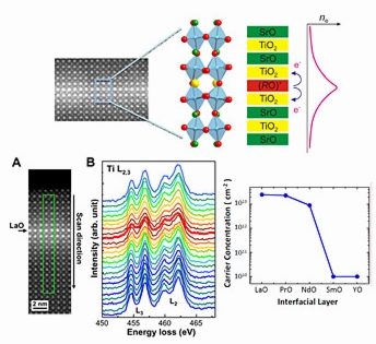 |
| Top row: An atomic image of strontium titanate with one single rare-earth (R) -oxygen layer in the middle. The structure model is shown in the middle, where red is oxygen, green is strontium, blue is titanium and yellow is the rare-earth element. The RO layer at the interface can donate electrons to neighboring atomic layers.
Bottom row: Atom-by-atom imaging and spectroscopy measurement of the electronic structure at a highly conductive interface where lanthanum oxide was inserted. The conductivity measurement shows a drastic difference in electron concentration at the interface for different R elements. |
Abstract:
Most people cross borders such as doorways or state lines without thinking much about it. Yet not all borders are places of limbo intended only for crossing. Some borders, like those between two materials that are brought together, are dynamic places where special things can happen.
Engineering Atomic Interfaces for New Electronics
Upton, NY | Posted on February 24th, 2011For an electron moving from one material toward the other, this space is where it can join other electrons, which together can create current, magnetism or even light.
A multi-institutional team has made fundamental discoveries at the border regions, called interfaces, between oxide materials. Led by University of Wisconsin-Madison Materials Science and Engineering Professor Chang-Beom Eom, the team has discovered how to manipulate electrons oxide interfaces by inserting a single layer of atoms. The researchers also have discovered unusual electron behaviors at these engineered interfaces.
Their work, which will be published February 18, 2011, in the journal Science, will allow researchers to further study and develop interfaces with a wide array of properties.
Eom's team blends theorists and experimentalists, including UW-Madison Physics Professor Mark Rzchowski and collaborators at the University of Nebraska-Lincoln, University of Michigan, Argonne National Laboratory and Brookhaven National Laboratory.
The researchers used two pieces of precisely grown strontium titanate, which is a type of oxide, or compound with oxygen as a fundamental element. Between the pieces, the researchers inserted a one-atom-thick layer of one of five rare-earth elements, which are important components in the electronics industry.
The team found that the rare-earth element layer creates an electron gas that has some interesting characteristics. The gas actually behaves more like an electron "liquid," since the electrons move more in tandem, or in correlation, than a gas normally does.
"If you take two materials, each has different characteristics, and if you put them together, at their interface you may find something unexpected," Eom says.
This research is the first demonstration of strong correlation among electrons at an oxide interface. The electron layer displayed distinct characteristics depending on the particular rare-earth element the team used. Materials with larger ionic radii, such as lanthanum, neodymium and praseodymium, are conducting, whereas materials with smaller radii, including samarium and yttrium, are insulating.
The insulating elements form an electron gas that can be compared to a thick liquid, somewhat like honey. The higher viscosity (basically, thickness) means the electrons can't move around as freely, making them more insulating. Conversely, the conducting elements form a gas that is a "liquid" more like gasoline; the viscosity is lower, so the electrons can move more freely and are better conductors.
Prior to this research, scientists knew extra electrons could reside at interfaces, but they didn't realize the complexity of how the electrons then behaved together at those interfaces.
The discovery of liquid-like behavior in the electron layer could open up an entire field of interfacial engineering for other scientists to explore, as well as new applications that take advantage of electron interactions. Since Eom and his colleagues developed an understanding of the basic physics behind these behaviors, their work could be expanded to create not only conductive or insulating interfaces, but also magnetic or optical ones.
Though scientists previously have looked at semiconductor interfaces, Eom's team is the first to specifically address those that use oxide interfaces to control conducting states with a single atomic layer. Oxides make up a class of materials including millions of compounds, and each has its own unique set of properties. The ability to manipulate various oxide interfaces could give rise to new generations of materials, electronics and other devices.
"This advancement could make a broad impact in fields even beyond physics, materials or chemistry," Eom says. "People can use the idea that an interface made from a single atomic layer of different ions can be used to create all kinds of properties."
####
About Brookhaven National Laboratory
One of ten national laboratories overseen and primarily funded by the Office of Science of the U.S. Department of Energy (DOE), Brookhaven National Laboratory conducts research in the physical, biomedical, and environmental sciences, as well as in energy technologies and national security. Brookhaven Lab also builds and operates major scientific facilities available to university, industry and government researchers. Brookhaven is operated and managed for DOE's Office of Science by Brookhaven Science Associates, a limited-liability company founded by the Research Foundation of State University of New York on behalf of Stony Brook University, the largest academic user of Laboratory facilities, and Battelle, a nonprofit, applied science and technology organization.
For more information, please click here
Contacts:
Written by:
Sandra Knisely
(608) 346-1463
Contact:
Chang-Beom Eom
(608) 263-6305
Brookhaven
Kendra Snyder
631-344-8191
or
Peter Genzer
631-344-3174
Copyright © Brookhaven National Laboratory
If you have a comment, please Contact us.Issuers of news releases, not 7th Wave, Inc. or Nanotechnology Now, are solely responsible for the accuracy of the content.
Bookmark:


| Related News Press |
News and information
![]() Simulating magnetization in a Heisenberg quantum spin chain April 5th, 2024
Simulating magnetization in a Heisenberg quantum spin chain April 5th, 2024
![]() NRL charters Navy�s quantum inertial navigation path to reduce drift April 5th, 2024
NRL charters Navy�s quantum inertial navigation path to reduce drift April 5th, 2024
![]() Discovery points path to flash-like memory for storing qubits: Rice find could hasten development of nonvolatile quantum memory April 5th, 2024
Discovery points path to flash-like memory for storing qubits: Rice find could hasten development of nonvolatile quantum memory April 5th, 2024
Laboratories
![]() A battery�s hopping ions remember where they�ve been: Seen in atomic detail, the seemingly smooth flow of ions through a battery�s electrolyte is surprisingly complicated February 16th, 2024
A battery�s hopping ions remember where they�ve been: Seen in atomic detail, the seemingly smooth flow of ions through a battery�s electrolyte is surprisingly complicated February 16th, 2024
![]() NRL discovers two-dimensional waveguides February 16th, 2024
NRL discovers two-dimensional waveguides February 16th, 2024
![]() Three-pronged approach discerns qualities of quantum spin liquids November 17th, 2023
Three-pronged approach discerns qualities of quantum spin liquids November 17th, 2023
Chip Technology
![]() Discovery points path to flash-like memory for storing qubits: Rice find could hasten development of nonvolatile quantum memory April 5th, 2024
Discovery points path to flash-like memory for storing qubits: Rice find could hasten development of nonvolatile quantum memory April 5th, 2024
![]() Utilizing palladium for addressing contact issues of buried oxide thin film transistors April 5th, 2024
Utilizing palladium for addressing contact issues of buried oxide thin film transistors April 5th, 2024
![]() HKUST researchers develop new integration technique for efficient coupling of III-V and silicon February 16th, 2024
HKUST researchers develop new integration technique for efficient coupling of III-V and silicon February 16th, 2024
Nanoelectronics
![]() Interdisciplinary: Rice team tackles the future of semiconductors Multiferroics could be the key to ultralow-energy computing October 6th, 2023
Interdisciplinary: Rice team tackles the future of semiconductors Multiferroics could be the key to ultralow-energy computing October 6th, 2023
![]() Key element for a scalable quantum computer: Physicists from Forschungszentrum J�lich and RWTH Aachen University demonstrate electron transport on a quantum chip September 23rd, 2022
Key element for a scalable quantum computer: Physicists from Forschungszentrum J�lich and RWTH Aachen University demonstrate electron transport on a quantum chip September 23rd, 2022
![]() Reduced power consumption in semiconductor devices September 23rd, 2022
Reduced power consumption in semiconductor devices September 23rd, 2022
![]() Atomic level deposition to extend Moore�s law and beyond July 15th, 2022
Atomic level deposition to extend Moore�s law and beyond July 15th, 2022
Discoveries
![]() Chemical reactions can scramble quantum information as well as black holes April 5th, 2024
Chemical reactions can scramble quantum information as well as black holes April 5th, 2024
![]() New micromaterial releases nanoparticles that selectively destroy cancer cells April 5th, 2024
New micromaterial releases nanoparticles that selectively destroy cancer cells April 5th, 2024
![]() Utilizing palladium for addressing contact issues of buried oxide thin film transistors April 5th, 2024
Utilizing palladium for addressing contact issues of buried oxide thin film transistors April 5th, 2024
Announcements
![]() NRL charters Navy�s quantum inertial navigation path to reduce drift April 5th, 2024
NRL charters Navy�s quantum inertial navigation path to reduce drift April 5th, 2024
![]() Discovery points path to flash-like memory for storing qubits: Rice find could hasten development of nonvolatile quantum memory April 5th, 2024
Discovery points path to flash-like memory for storing qubits: Rice find could hasten development of nonvolatile quantum memory April 5th, 2024
|
|
||
|
|
||
| The latest news from around the world, FREE | ||
|
|
||
|
|
||
| Premium Products | ||
|
|
||
|
Only the news you want to read!
Learn More |
||
|
|
||
|
Full-service, expert consulting
Learn More |
||
|
|
||