Home > Press > Seeing the Light
 |
| Scientists at Berkeley Lab�s Molecular Foundry have developed a web-based imaging toolkit designed for researchers studying plasmonic and photonic structures. This open-source software is available at www.nanohub.org. |
Abstract:
Berkeley Lab Scientists Bring Plasmonic Nanofields Into Focus
Seeing the Light
Berkeley, CA | Posted on February 7th, 2011In typical plasmonic devices, electromagnetic waves crowd into tiny metal structures, concentrating energy into nanoscale dimensions. Due to coupling of electronics and photonics in these metal nanostructures, plasmonic devices could be harnessed for high-speed data transmission or ultrafast detector arrays. However, studying plasmonic fields in nanoscale devices presents a real roadblock for scientists, as examining these structures inherently alters their behavior.
"Whether you use a laser or a light bulb, the wavelength of light is still too large to study plasmonic fields in nanostructures. What's more, most tools used to study plasmonic fields will alter the field distribution�the very behavior we hope to understand," says Jim Schuck, a staff scientist with Lawrence Berkeley National Laboratory (Berkeley Lab) who works in the Imaging and Manipulation of Nanostructures Facility at the Molecular Foundry.
Light microscopy plays a fundamental role in a scientist's repertoire: the technique is easy to use and doesn't inflict damage to a carefully crafted electronic circuit or delicate biological specimen. However, a typical nanoscale object of interest�such as a strand of DNA or a quantum dot�is well below the wavelength of visible light in size, which means the ability to distinguish one such object from another when they are closely spaced is lost. Scientists are now challenging this limit using �localization' techniques, which count the number of photons emanating from an object to help determine its position.
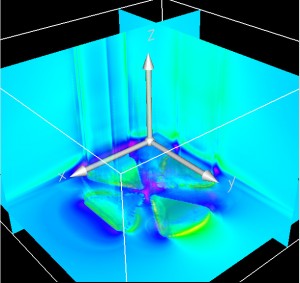
In previous work, Schuck and colleagues at the Molecular Foundry, a U.S. Department of Energy (DOE) Nanoscale Science Research Centers, engineered bowtie-shaped plasmonic devices designed to capture, filter and steer light at the nanoscale. These nano-color sorter devices served as antennae to focus and sort light in tiny spaces to a desired set of colors or energies�crucial for filters and other detectors.
In this latest advance, Schuck and his Berkeley Lab team used their innovative imaging concept to visualize plasmonic fields from these devices with nanoscale resolution. By imaging fluorescence from gold within the bowtie and maximizing the number of photons collected from their bowtie devices, the team was able to glean the position of plasmonic modes�oscillations of charge that result in optical resonance�just a few nanometers apart.
"We wondered whether there was a way to use light already present in our bowties�localized photons�to probe these fields and serve as a reporter," says Schuck. "Our technique is also sensitive to imperfections in the system, such as tiny structural flaws or size effects, suggesting we could use this technique to measure the performance of plasmonic devices in both research and development settings."
In parallel with Schuck's experimental findings, Jeff Neaton, Director of the Molecular Foundry 's Theory of Nanostructured Materials Facility and Alex McLeod, an undergraduate student working at the Foundry, developed a web-based toolkit, designed to calculate images of plasmonic devices with open-source software developed at Massachusetts Institute of Technology. For this study, the researchers simulated adjusting the structure of a double bowtie antenna by a few nanometers to study how changing the size and symmetry of a plasmonic antenna affects its optical properties.
"By shifting their structure by just a few nanometers, we can focus light at different positions inside the bowtie with remarkable certainty and predictability," said McLeod. "This work demonstrates that these nanoscale optical antennae resonate with light just as our simulations predict."
Useful for researchers studying plasmonic and photonic structures, this toolkit will be available for download on nanoHUB, a computational resource for nanoscience and technology created through the National Science Foundation's Network for Computational Nanotechnology.
"This work really exemplifies the very best of what the Molecular Foundry is about," said Neaton, who is also Acting Deputy Director of Berkeley Lab's Materials Sciences Division. "Three separate Foundry facilities�Imaging, Nanofabrication and Theory�collaborated on a significant advance in our understanding of how visible light can be localized, manipulated, and imaged at the nanoscale."
A paper reporting this research titled, "Non-perturbative visualization of nanoscale plasmonic field distributions via photon localization microscopy," appears in Physical Review Letters and is available to subscribers online. Co-authoring the paper with Schuck, McLeod and Neaton were Alexander Weber-Bargioni, Zhaoyu Zhang, Scott Dhuey, Bruce Harteneck and Stefano Cabrini.
Portions of this work at the Molecular Foundry were supported by DOE's Office of Science. Support for this work was also provided by the National Science Foundation through the Network for Computational Nanotechnology.
The Molecular Foundry is one of the five DOE Nanoscale Science Research Centers (NSRCs), national user facilities for interdisciplinary research at the nanoscale, supported by the DOE Office of Science. Together the NSRCs comprise a suite of complementary facilities that provide researchers with state-of-the-art capabilities to fabricate, process, characterize and model nanoscale materials, and constitute the largest infrastructure investment of the National Nanotechnology Initiative. The NSRCs are located at DOE's Argonne, Brookhaven, Lawrence Berkeley, Oak Ridge and Sandia and Los Alamos National Laboratories. For more information about the DOE NSRCs, please visit nano.energy.gov.
####
About Lawrence Berkeley National Laboratory
Lawrence Berkeley National Laboratory is a U.S. Department of Energy (DOE) national laboratory managed by the University of California for the DOE Office of Science. Berkeley Lab provides solutions to the world�s most urgent scientific challenges including sustainable energy, climate change, human health, and a better understanding of matter and force in the universe. It is a world leader in improving our lives through team science, advanced computing, and innovative technology.
For more information, please click here
Contacts:
Aditi Risbud
(510)486-4861
Copyright © Lawrence Berkeley National Laboratory
If you have a comment, please Contact us.Issuers of news releases, not 7th Wave, Inc. or Nanotechnology Now, are solely responsible for the accuracy of the content.
Bookmark:


| Related News Press |
News and information
![]() Simulating magnetization in a Heisenberg quantum spin chain April 5th, 2024
Simulating magnetization in a Heisenberg quantum spin chain April 5th, 2024
![]() NRL charters Navy�s quantum inertial navigation path to reduce drift April 5th, 2024
NRL charters Navy�s quantum inertial navigation path to reduce drift April 5th, 2024
![]() Discovery points path to flash-like memory for storing qubits: Rice find could hasten development of nonvolatile quantum memory April 5th, 2024
Discovery points path to flash-like memory for storing qubits: Rice find could hasten development of nonvolatile quantum memory April 5th, 2024
Software
![]() Visualizing nanoscale structures in real time: Open-source software enables researchers to see materials in 3D while they're still on the electron microscope August 19th, 2022
Visualizing nanoscale structures in real time: Open-source software enables researchers to see materials in 3D while they're still on the electron microscope August 19th, 2022
![]() Luisier wins SNSF Advanced Grant to develop simulation tools for nanoscale devices July 8th, 2022
Luisier wins SNSF Advanced Grant to develop simulation tools for nanoscale devices July 8th, 2022
![]() Oxford Instruments� Atomfab� system is production-qualified at a market-leading GaN power electronics device manufacturer December 17th, 2021
Oxford Instruments� Atomfab� system is production-qualified at a market-leading GaN power electronics device manufacturer December 17th, 2021
Govt.-Legislation/Regulation/Funding/Policy
![]() NRL charters Navy�s quantum inertial navigation path to reduce drift April 5th, 2024
NRL charters Navy�s quantum inertial navigation path to reduce drift April 5th, 2024
![]() Discovery points path to flash-like memory for storing qubits: Rice find could hasten development of nonvolatile quantum memory April 5th, 2024
Discovery points path to flash-like memory for storing qubits: Rice find could hasten development of nonvolatile quantum memory April 5th, 2024
![]() Chemical reactions can scramble quantum information as well as black holes April 5th, 2024
Chemical reactions can scramble quantum information as well as black holes April 5th, 2024
Possible Futures
![]() Discovery points path to flash-like memory for storing qubits: Rice find could hasten development of nonvolatile quantum memory April 5th, 2024
Discovery points path to flash-like memory for storing qubits: Rice find could hasten development of nonvolatile quantum memory April 5th, 2024
![]() With VECSELs towards the quantum internet Fraunhofer: IAF achieves record output power with VECSEL for quantum frequency converters April 5th, 2024
With VECSELs towards the quantum internet Fraunhofer: IAF achieves record output power with VECSEL for quantum frequency converters April 5th, 2024
Academic/Education
![]() Rice University launches Rice Synthetic Biology Institute to improve lives January 12th, 2024
Rice University launches Rice Synthetic Biology Institute to improve lives January 12th, 2024
![]() Multi-institution, $4.6 million NSF grant to fund nanotechnology training September 9th, 2022
Multi-institution, $4.6 million NSF grant to fund nanotechnology training September 9th, 2022
Announcements
![]() NRL charters Navy�s quantum inertial navigation path to reduce drift April 5th, 2024
NRL charters Navy�s quantum inertial navigation path to reduce drift April 5th, 2024
![]() Discovery points path to flash-like memory for storing qubits: Rice find could hasten development of nonvolatile quantum memory April 5th, 2024
Discovery points path to flash-like memory for storing qubits: Rice find could hasten development of nonvolatile quantum memory April 5th, 2024
Tools
![]() Ferroelectrically modulate the Fermi level of graphene oxide to enhance SERS response November 3rd, 2023
Ferroelectrically modulate the Fermi level of graphene oxide to enhance SERS response November 3rd, 2023
![]() The USTC realizes In situ electron paramagnetic resonance spectroscopy using single nanodiamond sensors November 3rd, 2023
The USTC realizes In situ electron paramagnetic resonance spectroscopy using single nanodiamond sensors November 3rd, 2023
|
|
||
|
|
||
| The latest news from around the world, FREE | ||
|
|
||
|
|
||
| Premium Products | ||
|
|
||
|
Only the news you want to read!
Learn More |
||
|
|
||
|
Full-service, expert consulting
Learn More |
||
|
|
||