Home > Press > New way to grow microwires
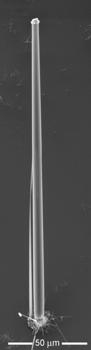 |
| This new technique for growing microwires can produce strands that are very long in relation to their diameter. The rounded �cap� at the wire�s top is a droplet of molten copper, while the wire itself is pure silicon. Image courtesy of Tonio Buonassisi |
Abstract:
Researchers find simple, inexpensive method to produce silicon wires for sensors, batteries and solar cells.
By David L. Chandler, MIT News Office
New way to grow microwires
Cambridge, MA | Posted on February 7th, 2011Microwires made of silicon � tiny wires with a thickness comparable to a human hair � have a wide range of possible uses, including the production of solar cells that can harvest much more sunlight for a given amount of material than a conventional solar cell made from a thin wafer of silicon crystal. Now researchers from MIT and Penn State have found a way of producing such wires in quantity in a highly controlled way that could be scaled up to an industrial-scale process, potentially leading to practical commercial applications.
Other ways of making such wires are already known, and prototypes of solar cells made from them have been produced by several researchers. But these methods have serious limitations, says Tonio Buonassisi, MIT professor of mechanical engineering and a co-author of a paper on the new work that was recently published online in the journal Small, and will soon appear in the print edition. Most require several extra manufacturing steps, provide little control over the exact sizes and spacing of the wires, and only work on flat surfaces. By contrast, the new process is simple yet allows precise control over the wire dimensions and spacing, and could theoretically be done on any kind of curved, 3-D surface.
Microwires are thought to be capable of reaching efficiencies close to those of conventional solar cells in converting sunlight to electricity, but because the wires are so tiny they would do so using only a small fraction of the amount of expensive silicon needed for the conventional cells, thus potentially achieving major reductions in cost.
In addition to microwires' potential use in solar cells, other researchers have proposed ways such microscopic wires could be used to build new kinds of transistors and integrated circuits, as well as electrodes for advanced batteries and certain kinds of environmental monitoring devices. For any of these ideas to be practical, however, there must be an efficient, scalable manufacturing method.
The new method involves heating and intentionally contaminating the surface of a silicon wafer with copper, which diffuses into the silicon. Then, when the silicon slowly cools, the copper diffuses out to form droplets on the surface. Then, when it is placed in an atmosphere of silicon tetrachloride gas, silicon microwires begin to grow outward wherever there is a copper droplet on the surface. Silicon in the gas dissolves into these copper droplets, and then after reaching a sufficient concentration begins to precipitate out at the bottom of the droplet, onto the silicon surface below. This buildup of silicon gradually elongates to form microwires each only about 10 to 20 micrometers (millionths of a meter) across, growing up from the surface. The whole process can be carried out repeatedly on an industrial manufacturing scale, Buonassisi says, or even could potentially be adapted to a continuous process.
The spacing of the wires is controlled by textures created on the surface � tiny dimples can form centers for the copper droplets � but the size of the wires is controlled by the temperatures used for the diffusion stage of the process. Thus, unlike in other production methods, the size and spacing of the wires can be controlled independently of each other, Buonassisi says.
The work done so far is just a proof of principle, he says, and more work remains to be done to find the best combinations of temperature profiles, copper concentrations and surface patterning for various applications, since the process allows for orders-of-magnitude differences in the size of the wires. For example, it remains to be determined what thickness and spacing of wires produces the most efficient solar cells. But this work demonstrates a potential for a kind of solar cell based on such wires that could significantly lower costs, both by allowing the use of lower grades of silicon (that is, less-highly refined), since the process of wire growth helps to purify the material, and by using much smaller amounts of it, since the tiny wires are made up of just a tiny fraction of the amount needed for conventional silicon crystal wafers. "This is still in a very early stage," Buonassisi says, because in deciding on a configuration for such a solar cell "there are so many things to optimize."
Michael Kelzenberg, a postdoctoral scholar at the California Institute of Technology who has spent the last five years doing research on silicon microwires, says that while others have used the copper-droplet technique for growing microwires, "What's really new here is the method of producing those liquid metal droplets." While others have had to place the droplets of molten copper on the silicon plate, requiring extra processing steps, "Buonassisi and his colleagues have shown that metal can be diffused into the growth substrate beforehand, and through careful heating and cooling, the metal droplets will actually form on their own � with the correct position and size."
Kelzenberg adds that his research group has recently demonstrated that silicon microwire solar cells can equal the efficiency of today's typical commercial solar cells. "I think the greatest challenge remaining is to show that this technique is more cost-effective or otherwise beneficial than other catalyst metal production methods," he says. But overall, he says, some version of silicon microwire technology "has the potential to enable dramatic cost reductions" of solar panels.
The paper was co-authored by Vidya Ganapati '10, doctoral student David Fenning, postdoctoral fellow Mariana Bertoni, and research specialist Alexandria Fecych, all in MIT's Department of Mechanical Engineering, and postdoctoral researcher Chito Kendrick and Professor Joan Redwing of Pennsylvania State University. The work was supported by the U.S. Department of Energy, the Chesonis Family Foundation and the National Science Foundation.
####
For more information, please click here
Copyright © MIT
If you have a comment, please Contact us.Issuers of news releases, not 7th Wave, Inc. or Nanotechnology Now, are solely responsible for the accuracy of the content.
Bookmark:


| Related News Press |
News and information
![]() Simulating magnetization in a Heisenberg quantum spin chain April 5th, 2024
Simulating magnetization in a Heisenberg quantum spin chain April 5th, 2024
![]() NRL charters Navy�s quantum inertial navigation path to reduce drift April 5th, 2024
NRL charters Navy�s quantum inertial navigation path to reduce drift April 5th, 2024
![]() Discovery points path to flash-like memory for storing qubits: Rice find could hasten development of nonvolatile quantum memory April 5th, 2024
Discovery points path to flash-like memory for storing qubits: Rice find could hasten development of nonvolatile quantum memory April 5th, 2024
Possible Futures
![]() Discovery points path to flash-like memory for storing qubits: Rice find could hasten development of nonvolatile quantum memory April 5th, 2024
Discovery points path to flash-like memory for storing qubits: Rice find could hasten development of nonvolatile quantum memory April 5th, 2024
![]() With VECSELs towards the quantum internet Fraunhofer: IAF achieves record output power with VECSEL for quantum frequency converters April 5th, 2024
With VECSELs towards the quantum internet Fraunhofer: IAF achieves record output power with VECSEL for quantum frequency converters April 5th, 2024
Academic/Education
![]() Rice University launches Rice Synthetic Biology Institute to improve lives January 12th, 2024
Rice University launches Rice Synthetic Biology Institute to improve lives January 12th, 2024
![]() Multi-institution, $4.6 million NSF grant to fund nanotechnology training September 9th, 2022
Multi-institution, $4.6 million NSF grant to fund nanotechnology training September 9th, 2022
Sensors
Discoveries
![]() Chemical reactions can scramble quantum information as well as black holes April 5th, 2024
Chemical reactions can scramble quantum information as well as black holes April 5th, 2024
![]() New micromaterial releases nanoparticles that selectively destroy cancer cells April 5th, 2024
New micromaterial releases nanoparticles that selectively destroy cancer cells April 5th, 2024
![]() Utilizing palladium for addressing contact issues of buried oxide thin film transistors April 5th, 2024
Utilizing palladium for addressing contact issues of buried oxide thin film transistors April 5th, 2024
Announcements
![]() NRL charters Navy�s quantum inertial navigation path to reduce drift April 5th, 2024
NRL charters Navy�s quantum inertial navigation path to reduce drift April 5th, 2024
![]() Discovery points path to flash-like memory for storing qubits: Rice find could hasten development of nonvolatile quantum memory April 5th, 2024
Discovery points path to flash-like memory for storing qubits: Rice find could hasten development of nonvolatile quantum memory April 5th, 2024
Battery Technology/Capacitors/Generators/Piezoelectrics/Thermoelectrics/Energy storage
![]() What heat can tell us about battery chemistry: using the Peltier effect to study lithium-ion cells March 8th, 2024
What heat can tell us about battery chemistry: using the Peltier effect to study lithium-ion cells March 8th, 2024
![]() A battery�s hopping ions remember where they�ve been: Seen in atomic detail, the seemingly smooth flow of ions through a battery�s electrolyte is surprisingly complicated February 16th, 2024
A battery�s hopping ions remember where they�ve been: Seen in atomic detail, the seemingly smooth flow of ions through a battery�s electrolyte is surprisingly complicated February 16th, 2024
Research partnerships
![]() Discovery points path to flash-like memory for storing qubits: Rice find could hasten development of nonvolatile quantum memory April 5th, 2024
Discovery points path to flash-like memory for storing qubits: Rice find could hasten development of nonvolatile quantum memory April 5th, 2024
![]() Researchers� approach may protect quantum computers from attacks March 8th, 2024
Researchers� approach may protect quantum computers from attacks March 8th, 2024
![]() 'Sudden death' of quantum fluctuations defies current theories of superconductivity: Study challenges the conventional wisdom of superconducting quantum transitions January 12th, 2024
'Sudden death' of quantum fluctuations defies current theories of superconductivity: Study challenges the conventional wisdom of superconducting quantum transitions January 12th, 2024
Solar/Photovoltaic
![]() Development of zinc oxide nanopagoda array photoelectrode: photoelectrochemical water-splitting hydrogen production January 12th, 2024
Development of zinc oxide nanopagoda array photoelectrode: photoelectrochemical water-splitting hydrogen production January 12th, 2024
![]() Shedding light on unique conduction mechanisms in a new type of perovskite oxide November 17th, 2023
Shedding light on unique conduction mechanisms in a new type of perovskite oxide November 17th, 2023
![]() Inverted perovskite solar cell breaks 25% efficiency record: Researchers improve cell efficiency using a combination of molecules to address different November 17th, 2023
Inverted perovskite solar cell breaks 25% efficiency record: Researchers improve cell efficiency using a combination of molecules to address different November 17th, 2023
![]() Charged �molecular beasts� the basis for new compounds: Researchers at Leipzig University use �aggressive� fragments of molecular ions for chemical synthesis November 3rd, 2023
Charged �molecular beasts� the basis for new compounds: Researchers at Leipzig University use �aggressive� fragments of molecular ions for chemical synthesis November 3rd, 2023
|
|
||
|
|
||
| The latest news from around the world, FREE | ||
|
|
||
|
|
||
| Premium Products | ||
|
|
||
|
Only the news you want to read!
Learn More |
||
|
|
||
|
Full-service, expert consulting
Learn More |
||
|
|
||