Home > Press > Engineers grow nanolasers on silicon, pave way for on-chip photonics
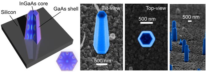 |
| Shown is a schematic (left) and various scanning electron microscope images of nanolasers grown directly on a silicon surface. The achievement could lead to a new class of optoelectronic chips. (Courtesy Connie Chang-Hasnain Group) |
Abstract:
Engineers at the University of California, Berkeley, have found a way to grow nanolasers directly onto a silicon surface, an achievement that could lead to a new class of faster, more efficient microprocessors, as well as to powerful biochemical sensors that use optoelectronic chips.
They describe their work in a paper to be published Feb. 6 in an advanced online issue of the journal Nature Photonics.
By Sarah Yang
Engineers grow nanolasers on silicon, pave way for on-chip photonics
Berkeley, CA | Posted on February 6th, 2011"Our results impact a broad spectrum of scientific fields, including materials science, transistor technology, laser science, optoelectronics and optical physics," said the study's principal investigator, Connie Chang-Hasnain, UC Berkeley professor of electrical engineering and computer sciences.
The increasing performance demands of electronics have sent researchers in search of better ways to harness the inherent ability of light particles to carry far more data than electrical signals can. Optical interconnects are seen as a solution to overcoming the communications bottleneck within and between computer chips.
Because silicon, the material that forms the foundation of modern electronics, is extremely deficient at generating light, engineers have turned to another class of materials known as III-V (pronounced "three-five") semiconductors to create light-based components such as light-emitting diodes (LEDs) and lasers.
But the researchers pointed out that marrying III-V with silicon to create a single optoelectronic chip has been problematic. For one, the atomic structures of the two materials are mismatched.
"Growing III-V semiconductor films on silicon is like forcing two incongruent puzzle pieces together," said study lead author Roger Chen, a UC Berkeley graduate student in electrical engineering and computer sciences. "It can be done, but the material gets damaged in the process."
Moreover, the manufacturing industry is set up for the production of silicon-based materials, so for practical reasons, the goal has been to integrate the fabrication of III-V devices into the existing infrastructure, the researchers said.
"Today's massive silicon electronics infrastructure is extremely difficult to change for both economic and technological reasons, so compatibility with silicon fabrication is critical," said Chang-Hasnain. "One problem is that growth of III-V semiconductors has traditionally involved high temperatures - 700 degrees Celsius or more - that would destroy the electronics. Meanwhile, other integration approaches have not been scalable."
The UC Berkeley researchers overcame this limitation by finding a way to grow nanopillars made of indium gallium arsenide, a III-V material, onto a silicon surface at the relatively cool temperature of 400 degrees Celsius.
"Working at nanoscale levels has enabled us to grow high quality III-V materials at low temperatures such that silicon electronics can retain their functionality," said Chen.
The researchers used metal-organic chemical vapor deposition to grow the nanopillars on the silicon. "This technique is potentially mass manufacturable, since such a system is already used commercially to make thin film solar cells and light emitting diodes," said Chang-Hasnain.
Once the nanopillar was made, the researchers showed that it could generate near infrared laser light - a wavelength of about 950 nanometers - at room temperature. The hexagonal geometry dictated by the crystal structure of the nanopillars creates a new, efficient, light-trapping optical cavity. Light circulates up and down the structure in a helical fashion and amplifies via this optical feedback mechanism.
The unique approach of growing nanolasers directly onto silicon could lead to highly efficient silicon photonics, the researchers said. They noted that the miniscule dimensions of the nanopillars - smaller than one wavelength on each side, in some cases - make it possible to pack them into small spaces with the added benefit of consuming very little energy
"Ultimately, this technique may provide a powerful and new avenue for engineering on-chip nanophotonic devices such as lasers, photodetectors, modulators and solar cells," said Chen.
"This is the first bottom-up integration of III-V nanolasers onto silicon chips using a growth process compatible with the CMOS (complementary metal oxide semiconductor) technology now used to make integrated circuits," said Chang-Hasnain. "This research has the potential to catalyze an optoelectronics revolution in computing, communications, displays and optical signal processing. In the future, we expect to improve the characteristics of these lasers and ultimately control them electronically for a powerful marriage between photonic and electronic devices."
The Defense Advanced Research Projects Agency and a Department of Defense National Security Science and Engineering Faculty Fellowship helped support this research.
####
For more information, please click here
Contacts:
Connie Chang-Hasnain
(650) 799-7355
Roger Chen
(508) 561-8213
Copyright © University of California, Berkeley
If you have a comment, please Contact us.Issuers of news releases, not 7th Wave, Inc. or Nanotechnology Now, are solely responsible for the accuracy of the content.
Bookmark:


| Related News Press |
News and information
![]() Simulating magnetization in a Heisenberg quantum spin chain April 5th, 2024
Simulating magnetization in a Heisenberg quantum spin chain April 5th, 2024
![]() NRL charters Navy�s quantum inertial navigation path to reduce drift April 5th, 2024
NRL charters Navy�s quantum inertial navigation path to reduce drift April 5th, 2024
![]() Discovery points path to flash-like memory for storing qubits: Rice find could hasten development of nonvolatile quantum memory April 5th, 2024
Discovery points path to flash-like memory for storing qubits: Rice find could hasten development of nonvolatile quantum memory April 5th, 2024
Govt.-Legislation/Regulation/Funding/Policy
![]() NRL charters Navy�s quantum inertial navigation path to reduce drift April 5th, 2024
NRL charters Navy�s quantum inertial navigation path to reduce drift April 5th, 2024
![]() Discovery points path to flash-like memory for storing qubits: Rice find could hasten development of nonvolatile quantum memory April 5th, 2024
Discovery points path to flash-like memory for storing qubits: Rice find could hasten development of nonvolatile quantum memory April 5th, 2024
![]() Chemical reactions can scramble quantum information as well as black holes April 5th, 2024
Chemical reactions can scramble quantum information as well as black holes April 5th, 2024
Possible Futures
![]() Discovery points path to flash-like memory for storing qubits: Rice find could hasten development of nonvolatile quantum memory April 5th, 2024
Discovery points path to flash-like memory for storing qubits: Rice find could hasten development of nonvolatile quantum memory April 5th, 2024
![]() With VECSELs towards the quantum internet Fraunhofer: IAF achieves record output power with VECSEL for quantum frequency converters April 5th, 2024
With VECSELs towards the quantum internet Fraunhofer: IAF achieves record output power with VECSEL for quantum frequency converters April 5th, 2024
Academic/Education
![]() Rice University launches Rice Synthetic Biology Institute to improve lives January 12th, 2024
Rice University launches Rice Synthetic Biology Institute to improve lives January 12th, 2024
![]() Multi-institution, $4.6 million NSF grant to fund nanotechnology training September 9th, 2022
Multi-institution, $4.6 million NSF grant to fund nanotechnology training September 9th, 2022
Sensors
Discoveries
![]() Chemical reactions can scramble quantum information as well as black holes April 5th, 2024
Chemical reactions can scramble quantum information as well as black holes April 5th, 2024
![]() New micromaterial releases nanoparticles that selectively destroy cancer cells April 5th, 2024
New micromaterial releases nanoparticles that selectively destroy cancer cells April 5th, 2024
![]() Utilizing palladium for addressing contact issues of buried oxide thin film transistors April 5th, 2024
Utilizing palladium for addressing contact issues of buried oxide thin film transistors April 5th, 2024
Announcements
![]() NRL charters Navy�s quantum inertial navigation path to reduce drift April 5th, 2024
NRL charters Navy�s quantum inertial navigation path to reduce drift April 5th, 2024
![]() Discovery points path to flash-like memory for storing qubits: Rice find could hasten development of nonvolatile quantum memory April 5th, 2024
Discovery points path to flash-like memory for storing qubits: Rice find could hasten development of nonvolatile quantum memory April 5th, 2024
Nanobiotechnology
![]() New micromaterial releases nanoparticles that selectively destroy cancer cells April 5th, 2024
New micromaterial releases nanoparticles that selectively destroy cancer cells April 5th, 2024
![]() Good as gold - improving infectious disease testing with gold nanoparticles April 5th, 2024
Good as gold - improving infectious disease testing with gold nanoparticles April 5th, 2024
![]() Researchers develop artificial building blocks of life March 8th, 2024
Researchers develop artificial building blocks of life March 8th, 2024
Photonics/Optics/Lasers
![]() With VECSELs towards the quantum internet Fraunhofer: IAF achieves record output power with VECSEL for quantum frequency converters April 5th, 2024
With VECSELs towards the quantum internet Fraunhofer: IAF achieves record output power with VECSEL for quantum frequency converters April 5th, 2024
![]() Nanoscale CL thermometry with lanthanide-doped heavy-metal oxide in TEM March 8th, 2024
Nanoscale CL thermometry with lanthanide-doped heavy-metal oxide in TEM March 8th, 2024
![]() Optically trapped quantum droplets of light can bind together to form macroscopic complexes March 8th, 2024
Optically trapped quantum droplets of light can bind together to form macroscopic complexes March 8th, 2024
![]() HKUST researchers develop new integration technique for efficient coupling of III-V and silicon February 16th, 2024
HKUST researchers develop new integration technique for efficient coupling of III-V and silicon February 16th, 2024
Solar/Photovoltaic
![]() Development of zinc oxide nanopagoda array photoelectrode: photoelectrochemical water-splitting hydrogen production January 12th, 2024
Development of zinc oxide nanopagoda array photoelectrode: photoelectrochemical water-splitting hydrogen production January 12th, 2024
![]() Shedding light on unique conduction mechanisms in a new type of perovskite oxide November 17th, 2023
Shedding light on unique conduction mechanisms in a new type of perovskite oxide November 17th, 2023
![]() Inverted perovskite solar cell breaks 25% efficiency record: Researchers improve cell efficiency using a combination of molecules to address different November 17th, 2023
Inverted perovskite solar cell breaks 25% efficiency record: Researchers improve cell efficiency using a combination of molecules to address different November 17th, 2023
![]() Charged �molecular beasts� the basis for new compounds: Researchers at Leipzig University use �aggressive� fragments of molecular ions for chemical synthesis November 3rd, 2023
Charged �molecular beasts� the basis for new compounds: Researchers at Leipzig University use �aggressive� fragments of molecular ions for chemical synthesis November 3rd, 2023
|
|
||
|
|
||
| The latest news from around the world, FREE | ||
|
|
||
|
|
||
| Premium Products | ||
|
|
||
|
Only the news you want to read!
Learn More |
||
|
|
||
|
Full-service, expert consulting
Learn More |
||
|
|
||