Home > Press > EU-funded team puts new semi-conductor material to the test
 |
Abstract:
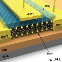
The electronic chips of the future might not be made of silicon or even graphene but of a material called molybdenite (MoS2). EU-funded research presented in the journal Nature Nanotechnology demonstrates that molybdenite is a highly effective semi-conductor that could be used to make transistors both smaller and more energy efficient.
EU-funded team puts new semi-conductor material to the test
EU | Posted on February 1st, 2011EU support for the work came from the 5-year FLATRONICS ('Electronic devices based on nanolayers') project, a EUR 1.8 million European Research Council (ERC) Starting Grant awarded to Professor Andras Kis of the Laboratory of Nanoscale Electronics and Structures (LANES) at the Ecole Polytechnique F�d�rale de Lausanne (EPFL) in Switzerland in 2009. ERC grants are channelled through the Ideas Programme of the Seventh Framework Programme (FP7).
Molybdenite is a mineral readily available in nature. Currently its main uses are as an element in steel alloys and as an additive in lubricants. Until now, its potential as a semi-conductor has remained largely unexplored.
'It's a two-dimensional material, very thin and easy to use in nanotechnology,' says Professor Kis, who led the current study. 'It has real potential in the fabrication of very small transistors, light-emitting diodes (LEDs) and solar cells.'
According to Professor Kis and his colleagues, molybdenite offers significant advantages over silicon, which is widely used in electronics, and graphene, which is the most widely studied two-dimensional material and is commonly viewed as the electronics material of the future.
Silicon is a three-dimensional material, and so is more voluminous than molybdenite that can be fabricated in monolayers. 'In a 0.65-nanometre-thick sheet of MoS2, the electrons can move around as easily as in a 2-nanometre-thick sheet of silicon, but it's not currently possible to fabricate a sheet of silicon as thin as a monolayer sheet of MoS2,' explains Professor Kis.
Furthermore, transistors based on molybdenite would consume 100,000 times less energy in their standby state than conventional silicon transistors. This is because turning a transistor on and off requires a semi-conductor material with a 'band gap'. In physics, 'bands' are used as a way of describing the energy of electrons in a material. In semi-conductors, the term 'band gap' refers to the electron-free spaces between these bands. If the gap is neither too big nor too small, some electrons can jump across the gap, thereby offering researchers a way of controlling the electrical behaviour of the material and turning it on and off. Molybdenite has a 1.8 electron-volt band gap, making it ideal for turning transistors on and off.
Molybdenite's band gap also gives it the edge over graphene, which does not have a band gap in its pristine state. Although it is possible to make graphene that has a band gap, this increases the fabrication complexity and causes other problems.
'Our results provide an important step towards the realization of electronics and low-standby-power integrated circuits based on two-dimensional materials. Being a thin, transparent semiconducting material, MoS2 monolayers also present a wealth of new opportunities in areas that include mesoscopic physics, optoelectronics and energy harvesting,' the researchers conclude.
'With the possibility of fabricating large-area circuits using solution-based processing, our finding could be important for producing electronic devices that could combine the ease of processing associated with organic conductors with performance figures commonly associated with silicon-based electronics.'
For more information, please visit:
Ecole Polytechnique F�d�rale de Lausanne (EPFL): www.epfl.ch
Nature Nanotechnology: www.nature.com/naturenanotechnology
European Research Council (ERC): erc.europa.eu
####
For more information, please click here
Copyright © CORDIS
If you have a comment, please Contact us.Issuers of news releases, not 7th Wave, Inc. or Nanotechnology Now, are solely responsible for the accuracy of the content.
Bookmark:


| Related News Press |
News and information
![]() Simulating magnetization in a Heisenberg quantum spin chain April 5th, 2024
Simulating magnetization in a Heisenberg quantum spin chain April 5th, 2024
![]() NRL charters Navy�s quantum inertial navigation path to reduce drift April 5th, 2024
NRL charters Navy�s quantum inertial navigation path to reduce drift April 5th, 2024
![]() Discovery points path to flash-like memory for storing qubits: Rice find could hasten development of nonvolatile quantum memory April 5th, 2024
Discovery points path to flash-like memory for storing qubits: Rice find could hasten development of nonvolatile quantum memory April 5th, 2024
![]() Good as gold - improving infectious disease testing with gold nanoparticles April 5th, 2024
Good as gold - improving infectious disease testing with gold nanoparticles April 5th, 2024
Display technology/LEDs/SS Lighting/OLEDs
![]() Utilizing palladium for addressing contact issues of buried oxide thin film transistors April 5th, 2024
Utilizing palladium for addressing contact issues of buried oxide thin film transistors April 5th, 2024
![]() Light guide plate based on perovskite nanocomposites November 3rd, 2023
Light guide plate based on perovskite nanocomposites November 3rd, 2023
![]() Simple ballpoint pen can write custom LEDs August 11th, 2023
Simple ballpoint pen can write custom LEDs August 11th, 2023
Possible Futures
![]() Discovery points path to flash-like memory for storing qubits: Rice find could hasten development of nonvolatile quantum memory April 5th, 2024
Discovery points path to flash-like memory for storing qubits: Rice find could hasten development of nonvolatile quantum memory April 5th, 2024
![]() With VECSELs towards the quantum internet Fraunhofer: IAF achieves record output power with VECSEL for quantum frequency converters April 5th, 2024
With VECSELs towards the quantum internet Fraunhofer: IAF achieves record output power with VECSEL for quantum frequency converters April 5th, 2024
Academic/Education
![]() Rice University launches Rice Synthetic Biology Institute to improve lives January 12th, 2024
Rice University launches Rice Synthetic Biology Institute to improve lives January 12th, 2024
![]() Multi-institution, $4.6 million NSF grant to fund nanotechnology training September 9th, 2022
Multi-institution, $4.6 million NSF grant to fund nanotechnology training September 9th, 2022
Chip Technology
![]() Discovery points path to flash-like memory for storing qubits: Rice find could hasten development of nonvolatile quantum memory April 5th, 2024
Discovery points path to flash-like memory for storing qubits: Rice find could hasten development of nonvolatile quantum memory April 5th, 2024
![]() Utilizing palladium for addressing contact issues of buried oxide thin film transistors April 5th, 2024
Utilizing palladium for addressing contact issues of buried oxide thin film transistors April 5th, 2024
![]() HKUST researchers develop new integration technique for efficient coupling of III-V and silicon February 16th, 2024
HKUST researchers develop new integration technique for efficient coupling of III-V and silicon February 16th, 2024
Nanoelectronics
![]() Interdisciplinary: Rice team tackles the future of semiconductors Multiferroics could be the key to ultralow-energy computing October 6th, 2023
Interdisciplinary: Rice team tackles the future of semiconductors Multiferroics could be the key to ultralow-energy computing October 6th, 2023
![]() Key element for a scalable quantum computer: Physicists from Forschungszentrum J�lich and RWTH Aachen University demonstrate electron transport on a quantum chip September 23rd, 2022
Key element for a scalable quantum computer: Physicists from Forschungszentrum J�lich and RWTH Aachen University demonstrate electron transport on a quantum chip September 23rd, 2022
![]() Reduced power consumption in semiconductor devices September 23rd, 2022
Reduced power consumption in semiconductor devices September 23rd, 2022
![]() Atomic level deposition to extend Moore�s law and beyond July 15th, 2022
Atomic level deposition to extend Moore�s law and beyond July 15th, 2022
Announcements
![]() NRL charters Navy�s quantum inertial navigation path to reduce drift April 5th, 2024
NRL charters Navy�s quantum inertial navigation path to reduce drift April 5th, 2024
![]() Discovery points path to flash-like memory for storing qubits: Rice find could hasten development of nonvolatile quantum memory April 5th, 2024
Discovery points path to flash-like memory for storing qubits: Rice find could hasten development of nonvolatile quantum memory April 5th, 2024
Solar/Photovoltaic
![]() Development of zinc oxide nanopagoda array photoelectrode: photoelectrochemical water-splitting hydrogen production January 12th, 2024
Development of zinc oxide nanopagoda array photoelectrode: photoelectrochemical water-splitting hydrogen production January 12th, 2024
![]() Shedding light on unique conduction mechanisms in a new type of perovskite oxide November 17th, 2023
Shedding light on unique conduction mechanisms in a new type of perovskite oxide November 17th, 2023
![]() Inverted perovskite solar cell breaks 25% efficiency record: Researchers improve cell efficiency using a combination of molecules to address different November 17th, 2023
Inverted perovskite solar cell breaks 25% efficiency record: Researchers improve cell efficiency using a combination of molecules to address different November 17th, 2023
![]() Charged �molecular beasts� the basis for new compounds: Researchers at Leipzig University use �aggressive� fragments of molecular ions for chemical synthesis November 3rd, 2023
Charged �molecular beasts� the basis for new compounds: Researchers at Leipzig University use �aggressive� fragments of molecular ions for chemical synthesis November 3rd, 2023
|
|
||
|
|
||
| The latest news from around the world, FREE | ||
|
|
||
|
|
||
| Premium Products | ||
|
|
||
|
Only the news you want to read!
Learn More |
||
|
|
||
|
Full-service, expert consulting
Learn More |
||
|
|
||