Home > Press > CAMECA Unveils News Semiconductor Metrology Tool
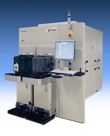 |
| Cameca EX-300 LEXES metrology tool |
Abstract:
Versatile Metrology Tool for Front-End Process Control Of 22nm Technology Nodes and Beyond
CAMECA Unveils News Semiconductor Metrology Tool
Gennevillers, France | Posted on January 27th, 2011CAMECA, a world leader in scientific instrumentation and metrology solutions for semiconductor labs and fabs, has unveiled the latest addition to its line of high-end metrology systems-the EX-300 metrology tool targeted for front-end process control of 22 nm technology nodes and beyond.
"CAMECA is very proud to introduce the EX-300," notes Dr. Michel Schuhmacher, CAMECA Vice President and Chief Technical Officer. "This highly versatile metrology tool benefits from CAMECA's 10-years of experience with LEXES (Low-energy Electron induced X-ray Emission Spectrometry) technology."
"We are convinced that the EX-300 will become the metrology tool of choice for semiconductor fabs integrating new challenging processes," adds Dr. Schuhmacher. "The EX-300 offers unique capabilities for front-end compositional control at and near the surface. The instrument targets front-end process control for 22nm technology nodes and performs metrology of patterned wafers down to 30x30�m."
The EX-300 utilizes LEXES, a unique surface probing technique pioneered by CAMECA. The technology is now well-established for addressing challenges in elemental composition, thickness determination and dopant dosimetry. With dozens of CAMECA LEXFAB 300 instruments currently installed at the top-ten semiconductor fabrication facilities worldwide, the technology is considered the standard for semiconductor R&D and ramping-up phases at the most advanced nodes as well as for high-volume production monitoring.
CAMECA optimized the performance of the EX-300 for challenging High K Metal Gate (HKMG), epitaxial layers such as Boron in Silcon Germanium(B:SiGe) and shallow implants, fulfilling requirements of both rapid device development and high-yield mass production. In addition, the instrument is designed to deliver enhanced long-term stability and minimize mean time to repair (MTTR).
####
About CAMECA
CAMECA has more than 50 years of experience in the design, manufacture and servicing of scientific instruments for material micro- and nano-analysis. Since pioneering Secondary Ion Mass Spectrometry (SIMS) and Electron Probe Microanalysis (EPMA) instrumentation in the 1950s, CAMECA has remained an undisputed world leader, while achieving numerous breakthrough innovations in such complementary techniques as LEXES and Atom Probe Tomography.
More recently CAMECA has evolved successfully from a provider of scientific instrumentation for the international research community to a provider of metrology solutions for the semiconductor industry. Headquartered near Paris, CAMECA has subsidiaries in China, Germany, Japan, Korea, Taiwan and the United States along with a global network of agents. Acquired in 2007 by AMETEK, Inc, a leading global manufacturer of electronic instrument and electromechanical products, CAMECA is now a unit of AMETEK�s Materials Analysis Division.
For more information, please click here
Contacts:
Marion Chopin
+33 (1) 43 34 62 00
Copyright © CAMECA
If you have a comment, please Contact us.Issuers of news releases, not 7th Wave, Inc. or Nanotechnology Now, are solely responsible for the accuracy of the content.
Bookmark:


| Related News Press |
News and information
![]() Simulating magnetization in a Heisenberg quantum spin chain April 5th, 2024
Simulating magnetization in a Heisenberg quantum spin chain April 5th, 2024
![]() NRL charters Navy�s quantum inertial navigation path to reduce drift April 5th, 2024
NRL charters Navy�s quantum inertial navigation path to reduce drift April 5th, 2024
![]() Discovery points path to flash-like memory for storing qubits: Rice find could hasten development of nonvolatile quantum memory April 5th, 2024
Discovery points path to flash-like memory for storing qubits: Rice find could hasten development of nonvolatile quantum memory April 5th, 2024
Chip Technology
![]() Discovery points path to flash-like memory for storing qubits: Rice find could hasten development of nonvolatile quantum memory April 5th, 2024
Discovery points path to flash-like memory for storing qubits: Rice find could hasten development of nonvolatile quantum memory April 5th, 2024
![]() Utilizing palladium for addressing contact issues of buried oxide thin film transistors April 5th, 2024
Utilizing palladium for addressing contact issues of buried oxide thin film transistors April 5th, 2024
![]() HKUST researchers develop new integration technique for efficient coupling of III-V and silicon February 16th, 2024
HKUST researchers develop new integration technique for efficient coupling of III-V and silicon February 16th, 2024
Memory Technology
![]() Utilizing palladium for addressing contact issues of buried oxide thin film transistors April 5th, 2024
Utilizing palladium for addressing contact issues of buried oxide thin film transistors April 5th, 2024
![]() Interdisciplinary: Rice team tackles the future of semiconductors Multiferroics could be the key to ultralow-energy computing October 6th, 2023
Interdisciplinary: Rice team tackles the future of semiconductors Multiferroics could be the key to ultralow-energy computing October 6th, 2023
![]() Researchers discover materials exhibiting huge magnetoresistance June 9th, 2023
Researchers discover materials exhibiting huge magnetoresistance June 9th, 2023
Nanoelectronics
![]() Interdisciplinary: Rice team tackles the future of semiconductors Multiferroics could be the key to ultralow-energy computing October 6th, 2023
Interdisciplinary: Rice team tackles the future of semiconductors Multiferroics could be the key to ultralow-energy computing October 6th, 2023
![]() Key element for a scalable quantum computer: Physicists from Forschungszentrum J�lich and RWTH Aachen University demonstrate electron transport on a quantum chip September 23rd, 2022
Key element for a scalable quantum computer: Physicists from Forschungszentrum J�lich and RWTH Aachen University demonstrate electron transport on a quantum chip September 23rd, 2022
![]() Reduced power consumption in semiconductor devices September 23rd, 2022
Reduced power consumption in semiconductor devices September 23rd, 2022
![]() Atomic level deposition to extend Moore�s law and beyond July 15th, 2022
Atomic level deposition to extend Moore�s law and beyond July 15th, 2022
Announcements
![]() NRL charters Navy�s quantum inertial navigation path to reduce drift April 5th, 2024
NRL charters Navy�s quantum inertial navigation path to reduce drift April 5th, 2024
![]() Discovery points path to flash-like memory for storing qubits: Rice find could hasten development of nonvolatile quantum memory April 5th, 2024
Discovery points path to flash-like memory for storing qubits: Rice find could hasten development of nonvolatile quantum memory April 5th, 2024
Tools
![]() Ferroelectrically modulate the Fermi level of graphene oxide to enhance SERS response November 3rd, 2023
Ferroelectrically modulate the Fermi level of graphene oxide to enhance SERS response November 3rd, 2023
![]() The USTC realizes In situ electron paramagnetic resonance spectroscopy using single nanodiamond sensors November 3rd, 2023
The USTC realizes In situ electron paramagnetic resonance spectroscopy using single nanodiamond sensors November 3rd, 2023
|
|
||
|
|
||
| The latest news from around the world, FREE | ||
|
|
||
|
|
||
| Premium Products | ||
|
|
||
|
Only the news you want to read!
Learn More |
||
|
|
||
|
Full-service, expert consulting
Learn More |
||
|
|
||