Home > Press > Picosun develops green communication technologies aiming at erasing 13 million tons of CO2 emissions
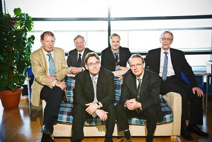 |
| Picosun Board of Directors: Professor Jorma Routti (left) - former Director General of EU Science Directorate, Professor Lauri Niinist� - recently awarded first ever GerALD prize, M.Sc Kustaa Poutiainen - Picosun Chairman and CEO, M.Sc Juhana Kostamo - Picosun Managing Director, Dr. Tuomo Suntola - inventor of ALD technology, and Mr. Sven Lindfors - Picosun CTO and world's most experienced designer of ALD systems. |
Abstract:
Picosun Oy, Finland-based global manufacturer of state-of-the-art Atomic Layer Deposition (ALD) systems, takes part in EPAMO, a major 13.3 million euro project aiming at reducing up to 1,700 Megawatts (MW) from the global energy consumption of wireless communication systems, such as mobile phone technology.
Picosun develops green communication technologies aiming at erasing 13 million tons of CO2 emissions
Espoo, Finland | Posted on January 17th, 2011Picosun is one of the eleven top-tier industrial and four leading research partners from Finland, Germany, the Netherlands, and Sweden forming the EPAMO partnership.
Endless increase in wireless traffic will congest global data transfer systems. Tomorrow there will be an increased number of frequency bands and advanced mobile phone standards supporting high data rates. According to estimates, the number of mobile phone base stations will grow from current five million to ten million by 2015 largely due to new communication infrastructure being built in the developing countries. This amount of base stations consumes some 15,000 Megawatts of power.
New technology developed through EPAMO will cut some 1,500 MW of this consumption alone. EPAMO's input into handset technology will add additional 140 MW of saved energy into the pool of tomorrow's greener communication systems. 1,640 MW is more than the electric power capacity of the very latest giant nuclear plant type, still under construction in Finland and France. Generating that amount of energy through the use of fossil fuels would release 12.9 million metric tons of carbon dioxide (CO2) into the environment every year.
EPAMO is based on the intent to create a new MEMS (Microelectromechanical Systems) technology platform which enables an RF (Radio Frequency) front-end architecture for both today's and next generation mobile communication systems including handsets and base stations. Developing a reconfigurable antenna concept will produce unrivalled performance, energy efficiency, degree of miniaturization and cost efficiency. This will be achieved by a holistic approach providing new advanced wafer materials and RF component designs, combining new thin film materials and thin film technologies with CMOS (Complementary Metal-Oxide-Semiconductor) solutions following a More than Moore Law approach (Moore's Law focuses on transistor density; More than Moore Law refers to system integration and revolutionary megafunction electronics).
EPAMO is coordinated by Dr. Thomas Metzger of EPCOS AG of Germany. EPCOS is the world leader in RF filters and global number two on module solutions for the RF front-end of mobile phones. EPCOS Netherlands N.V. hosts the development and business development of several RF system solutions like antenna tuners, tunable power amplifiers and smart RF front-ends for EPCOS.
"Main goal for EPAMO is the global mobile phone cluster, but the same antenna tuner technology will also enter into mobile IT devices like PDA (Personal Digital Assistant) mobile mini laptops, tablet computers and other such devices to increase and optimize the data throughput. For EPAMO products this will open another market, similar in size to the mobile phone industry potential," says Juhana Kostamo, Managing Director of Picosun.
Picosun will, as a part of EPAMO, develop advanced materials based on ALD and solve manufacturing process challenges concerning deposition of uniform and conformal thin films on substrates containing 3D structures and high aspect ratio TSVs (Through-Silicon Vias). "RF-MEMS become so miniscule in size and so complicated in structure that ALD offers the only feasible technology for RF-MEMS thin films. In view of this it is very fortunate that solving ALD related production challenges is the very area where Picosun has been leading the way lately," Mr. Kostamo says.
ENIAC JU (European Technology Platform on Nanoelectronics Joint Undertaking), a public-private partnership between the European Commission, 21 European countries and various nanoelectronics actors funds 2.2 M� of EPAMO budget. National public funding from the participating nations covers 5.5 M�, and 5.6 M� comes from EPAMO partners.
Global MEMS market will grow to more than 12.5 billion US$ by 2012. Of this, almost 1.2 billion will be RF-MEMS. Whilst the overall MEMS market will grow with a CAGR (Compound Annual Growth Rate) of 17% from 2008 to 2012, RF-MEMS is expected to have a CAGR of 45%, the highest of all MEMS sectors.
####
About Picosun
Picosun Oy is a global manufacturer of state-of-the-art ALD systems for micro- and nanotechnology applications. Picosun represents continuity for over three decades of ALD reactor design and manufacturing in Finland. Picosun is based in Espoo, Finland and has its US headquarters in Detroit, Michigan. SUNALE� ALD process tools are installed in various universities, research institutes and companies across four continents. Picosun Oy is a part of Stephen Industries Inc Oy.
Dr. Tuomo Suntola, inventor of ALD technology, is Member of the Board of Directors of Picosun. World�s most experienced ALD reactor designer Sven Lindfors is Picosun�s Chief Technology Officer and founder of the company. Picosun Oy is a part of Stephen Industries Inc Oy.
For more information, please click here
Contacts:
Picosun Oy, Mr. Juhana Kostamo, Managing Director
Tietotie 3, FI-02150 Espoo Finland
Tel. +358 50 321 1955
Fax. +358 20 722 7012;
e-mail: info (at) picosun.com
Copyright © Picosun Oy
If you have a comment, please Contact us.Issuers of news releases, not 7th Wave, Inc. or Nanotechnology Now, are solely responsible for the accuracy of the content.
Bookmark:


| Related News Press |
News and information
![]() Simulating magnetization in a Heisenberg quantum spin chain April 5th, 2024
Simulating magnetization in a Heisenberg quantum spin chain April 5th, 2024
![]() NRL charters Navy�s quantum inertial navigation path to reduce drift April 5th, 2024
NRL charters Navy�s quantum inertial navigation path to reduce drift April 5th, 2024
![]() Discovery points path to flash-like memory for storing qubits: Rice find could hasten development of nonvolatile quantum memory April 5th, 2024
Discovery points path to flash-like memory for storing qubits: Rice find could hasten development of nonvolatile quantum memory April 5th, 2024
![]() Good as gold - improving infectious disease testing with gold nanoparticles April 5th, 2024
Good as gold - improving infectious disease testing with gold nanoparticles April 5th, 2024
Thin films
![]() Utilizing palladium for addressing contact issues of buried oxide thin film transistors April 5th, 2024
Utilizing palladium for addressing contact issues of buried oxide thin film transistors April 5th, 2024
![]() Understanding the mechanism of non-uniform formation of diamond film on tools: Paving the way to a dry process with less environmental impact March 24th, 2023
Understanding the mechanism of non-uniform formation of diamond film on tools: Paving the way to a dry process with less environmental impact March 24th, 2023
![]() New study introduces the best graphite films: The work by Distinguished Professor Feng Ding at UNIST has been published in the October 2022 issue of Nature Nanotechnology November 4th, 2022
New study introduces the best graphite films: The work by Distinguished Professor Feng Ding at UNIST has been published in the October 2022 issue of Nature Nanotechnology November 4th, 2022
MEMS
Announcements
![]() NRL charters Navy�s quantum inertial navigation path to reduce drift April 5th, 2024
NRL charters Navy�s quantum inertial navigation path to reduce drift April 5th, 2024
![]() Discovery points path to flash-like memory for storing qubits: Rice find could hasten development of nonvolatile quantum memory April 5th, 2024
Discovery points path to flash-like memory for storing qubits: Rice find could hasten development of nonvolatile quantum memory April 5th, 2024
Energy
![]() Development of zinc oxide nanopagoda array photoelectrode: photoelectrochemical water-splitting hydrogen production January 12th, 2024
Development of zinc oxide nanopagoda array photoelectrode: photoelectrochemical water-splitting hydrogen production January 12th, 2024
![]() Shedding light on unique conduction mechanisms in a new type of perovskite oxide November 17th, 2023
Shedding light on unique conduction mechanisms in a new type of perovskite oxide November 17th, 2023
![]() Inverted perovskite solar cell breaks 25% efficiency record: Researchers improve cell efficiency using a combination of molecules to address different November 17th, 2023
Inverted perovskite solar cell breaks 25% efficiency record: Researchers improve cell efficiency using a combination of molecules to address different November 17th, 2023
![]() The efficient perovskite cells with a structured anti-reflective layer � another step towards commercialization on a wider scale October 6th, 2023
The efficient perovskite cells with a structured anti-reflective layer � another step towards commercialization on a wider scale October 6th, 2023
Alliances/Trade associations/Partnerships/Distributorships
![]() Chicago Quantum Exchange welcomes six new partners highlighting quantum technology solutions, from Chicago and beyond September 23rd, 2022
Chicago Quantum Exchange welcomes six new partners highlighting quantum technology solutions, from Chicago and beyond September 23rd, 2022
![]() University of Illinois Chicago joins Brookhaven Lab's Quantum Center June 10th, 2022
University of Illinois Chicago joins Brookhaven Lab's Quantum Center June 10th, 2022
Research partnerships
![]() Discovery points path to flash-like memory for storing qubits: Rice find could hasten development of nonvolatile quantum memory April 5th, 2024
Discovery points path to flash-like memory for storing qubits: Rice find could hasten development of nonvolatile quantum memory April 5th, 2024
![]() Researchers� approach may protect quantum computers from attacks March 8th, 2024
Researchers� approach may protect quantum computers from attacks March 8th, 2024
![]() 'Sudden death' of quantum fluctuations defies current theories of superconductivity: Study challenges the conventional wisdom of superconducting quantum transitions January 12th, 2024
'Sudden death' of quantum fluctuations defies current theories of superconductivity: Study challenges the conventional wisdom of superconducting quantum transitions January 12th, 2024
|
|
||
|
|
||
| The latest news from around the world, FREE | ||
|
|
||
|
|
||
| Premium Products | ||
|
|
||
|
Only the news you want to read!
Learn More |
||
|
|
||
|
Full-service, expert consulting
Learn More |
||
|
|
||