Home > Press > Plasmonics: From metallic foils to cancer treatment
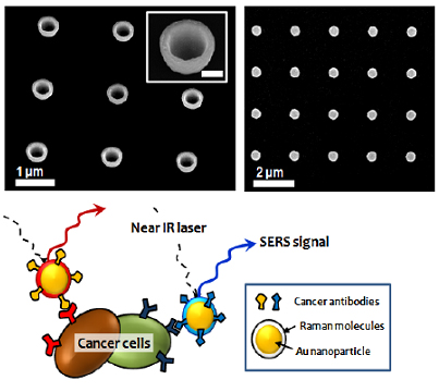 |
| Fig.1: (above) SEM images of nanoparticles fabricated for SERS by electron-beam lithography. (below) Illustration of multiplex cancer targeting by SERS nanoparticles encoded by Raman molecules and cancer antibodies. |
Abstract:
Highlight of STAM paper on plasmons in metallic nanostructures by Nagao et al.
Plasmonics: From metallic foils to cancer treatment
Tsukuba, Japan | Posted on January 12th, 2011In a timely review paper, scientists from Japan, Germany, and Spain provide a highly relevant overview of the history, physical interpretation and applications of plasmons in metallic nanostructures.
Tadaaki Nagao at the International Center for Materials Nanoarchitectonics (MANA), National Institute for Materials Science (NIMS) and colleagues in Germany and Spain present a review on plasmons in metallic nanomaterials. The article is published this week in the journal Science and Technology of Advanced Materials.
The authors provide an extensive overview of the properties of plasmons in nanomaterials with emphasis on pioneering work of Ruthemann and Lang on electron energy loss spectroscopy (EELS) of electron motion in thin metal foils; recent infrared analysis of nanoscale metallic nanorods and nanoislands produced by �top-down' photolithography; and the potential of metallic atomic wires for supporting plasmonic resonating modes. The review includes detailed explanations of plasmons for in vivo biosensing and nanoantennas.
A plasmon can be visualized as a collective oscillation of electronic �liquid' in metals, similar to waves in lake, which are collective mode of the water molecules. Furthermore, surface plasmons are such oscillations confined to the surfaces of metals, which display a strong interaction with light, leading to the formation of so-called �polaritons'. Futuristic applications of plasmons include ideal lenses and even invisibility cloaks.
Research in the 1940s by Ruthemann and Lang on electrons flowing in thin metal foils using EELS yielded the first experimental sign of the presence of the theoretically predicted �plasma oscillations' in metals. In 1957 Richie and colleagues predicted the existence of �surface localized' plasmons, which was confirmed by Powell and Swan by EELS a few years later. In the 1960s researchers determined optical dispersion curves using optical spectroscopy, thereby opening up the possibility of optical applications of plasmon structures.
In this review, Nagao and colleagues offer insights into optical applications of localized surface plasmons in structures produced by photolithography. Specific examples include metallic nanoantenna detectors�where resonant excitation of light leads to ultrahigh electromagnetic field enhancement owing to plasmon polaritons localized at the surface of nanostructures; and optical interactions between arrays of nanorods for �surface enhanced Raman scattering', which shows potential for in vivo biomolecular sensing. The authors also describe the fabrication of a prototype random-nanogap antenna for enhanced IR spectroscopy and in situ spectral monitoring of surface enhancement of infrared absorption during film growth.
Furthermore, the authors describe new trends in plasmonics research, in particular observation of plasmonic resonant modes in indium nanowires grown in ultrahigh vacuum on stepped silicon substrates. They predict that these nanowires will be used as building blocks for developing plasmonic devices of the future.
This review includes 86 references and 12 figures, providing an invaluable source of up-to-date information for newcomers and experts in this exciting field of research.
References and related websites
1. Tadaaki Nagao et al. Plasmons in nanoscale and atomic-scale system Science and Technology of Advanced Materials 11 (2010) No. 5, December. iopscience.iop.org/1468-6996/11/5/054506
Sci. Technol. Adv. Mater. Vol. 11 (2010) p. 054506 doi: 10.1088/1468-6996/11/5/054506
2. International Center for Materials Nanoarchitectonics (MANA), National Institute for Materials Science (NIMS), Tsukuba 305-0044, Japan www.nims.go.jp/eng/research/mana/index.html
3. Kirchhoff Institute for Physics, University of Heidelberg, Im Neuenheimer Feld 227,
D 69120, Heidelberg, Germany www.uni-heidelberg.de/index_e.html
4. Depto. de F�sica de Materiales, Facultad de Ciencias Quimicas, Universidad del Pais
Vasco, Apdo. 1072, 20080 San Sebastian/Donostia, Spain www.ehu.es/p200-shenhm/en
5. Donostia International Physics Center (DIPC), Paseo de Manuel Lardizabal 4, 20018
San Sebastian/Donostia, Spain dipc.ehu.es/
6. IKERBASQUE, Basque Foundation for Science, 48011 Bilbao, Spain www.ikerbasque.net
####
For more information, please click here
Contacts:
Media contacts:
National Institute for Materials Science, Tsukuba, Japan
Tel. +81-(0)29-859-2494
Copyright © MANA/NIMS
If you have a comment, please Contact us.Issuers of news releases, not 7th Wave, Inc. or Nanotechnology Now, are solely responsible for the accuracy of the content.
Bookmark:


| Related News Press |
News and information
![]() Simulating magnetization in a Heisenberg quantum spin chain April 5th, 2024
Simulating magnetization in a Heisenberg quantum spin chain April 5th, 2024
![]() NRL charters Navy�s quantum inertial navigation path to reduce drift April 5th, 2024
NRL charters Navy�s quantum inertial navigation path to reduce drift April 5th, 2024
![]() Discovery points path to flash-like memory for storing qubits: Rice find could hasten development of nonvolatile quantum memory April 5th, 2024
Discovery points path to flash-like memory for storing qubits: Rice find could hasten development of nonvolatile quantum memory April 5th, 2024
Academic/Education
![]() Rice University launches Rice Synthetic Biology Institute to improve lives January 12th, 2024
Rice University launches Rice Synthetic Biology Institute to improve lives January 12th, 2024
![]() Multi-institution, $4.6 million NSF grant to fund nanotechnology training September 9th, 2022
Multi-institution, $4.6 million NSF grant to fund nanotechnology training September 9th, 2022
Announcements
![]() NRL charters Navy�s quantum inertial navigation path to reduce drift April 5th, 2024
NRL charters Navy�s quantum inertial navigation path to reduce drift April 5th, 2024
![]() Discovery points path to flash-like memory for storing qubits: Rice find could hasten development of nonvolatile quantum memory April 5th, 2024
Discovery points path to flash-like memory for storing qubits: Rice find could hasten development of nonvolatile quantum memory April 5th, 2024
Research partnerships
![]() Discovery points path to flash-like memory for storing qubits: Rice find could hasten development of nonvolatile quantum memory April 5th, 2024
Discovery points path to flash-like memory for storing qubits: Rice find could hasten development of nonvolatile quantum memory April 5th, 2024
![]() Researchers� approach may protect quantum computers from attacks March 8th, 2024
Researchers� approach may protect quantum computers from attacks March 8th, 2024
![]() 'Sudden death' of quantum fluctuations defies current theories of superconductivity: Study challenges the conventional wisdom of superconducting quantum transitions January 12th, 2024
'Sudden death' of quantum fluctuations defies current theories of superconductivity: Study challenges the conventional wisdom of superconducting quantum transitions January 12th, 2024
|
|
||
|
|
||
| The latest news from around the world, FREE | ||
|
|
||
|
|
||
| Premium Products | ||
|
|
||
|
Only the news you want to read!
Learn More |
||
|
|
||
|
Full-service, expert consulting
Learn More |
||
|
|
||