Home > Press > Novel Nanomaterial System Will Help Create Materials Of The Future – For Applications From Semiconductors To Energy Conversion
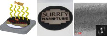 |
| A radical novel design concept for the growth of carbon nanotubes over large-area using a top-down CVD process allows high energy delivery to the catalyst whilst maintaining the substrate below 350 °C. Raman, EELS and HREM confirm the quality of the nanotubes is comparable with conventional catalytic nanotube growth at temperatures above 700 °C. † |
Abstract:
Materials to bypass semiconductor roadblocks are major target for first users
Novel Nanomaterial System Will Help Create Materials Of The Future – For Applications From Semiconductors To Energy Conversion
Newhaven, UK | Posted on January 10th, 2011Surrey NanoSystems announces the first sales of its innovative new nanomaterial growth system, the NanoGrowth-Catalyst, to the École Polytechnique of Montreal, and the University of Surrey's Advanced Technology Institute.
These leading research organizations have chosen the NanoGrowth-Catalyst as a platform for their work on materials including carbon nanotubes, silicon nanowires, graphene and nanoparticles for semiconductor, optical device and other applications. The growth system's multi-chamber design ensures the purest nanomaterial processing conditions by continuously maintaining the substrate under vacuum, from the deposition of catalysts to growth of materials.
One NanoGrowth-Catalyst system will be installed in Montreal, where it will support a wide range of research groups from the École Polytechnique and The University of Montreal studying topics including microelectronics, optoelectronics, and thin film physics.
This system will be populated with every major processing facility available including three processing chambers served by an automated handling system, and growth techniques including CVD, PECVD, nanoparticle deposition, sputtering, thermal annealing, and rapid thermal processing. It will also incorporate a unique form of rapid thermal growth for nanomaterials developed to prevent the agglomeration of catalyst particles. The configuration of the tool was specified by Professor Patrick Desjardins, Director of the École Polytechnique's Department of Engineering Physics.
One research group using the system will be the University of Montreal's chemistry department, led by Professor Richard Martel. The group's interests are very broad ranging, and include device-oriented programs looking at electronics, optoelectronics, sensing technologies and energy conversion, and fundamental research into the phenomena occurring at the interfaces of electroactive nanostructure materials - through projects including the deposition of controlled-size nanoparticles and passivation layers.
Dr Pierre Levesque of the University of Montreal's chemistry department comments: "We were looking for a very capable system that could support wide-ranging research, and which is easy to use. The very high-level software-controlled automation of nanomaterial processing offered by NanoGrowth-Catalyst gives us this versatility."
The Advanced Technology Institute (ATI) is a partner to Surrey NanoSystems and has already been using an earlier version of the NanoGrowth system for around four years to support its research into next-generation semiconductor and photonic device technologies. ATI is the first customer to receive the new NanoGrowth-Catalyst, and the system's advanced processing resources are now starting to play a role in its work. Facilities including the rapid infrared heating process and a water-cooled chuck are helping ATI to grow ordered carbon nanotube (CNT) structures while maintaining the substrate below 350 degrees C. Low temperature processing is critical as CNTs are typically grown at around 700 degrees C - a level that is incompatible with CMOS semiconductor fabrication. This pioneering semiconductor-related work is currently the subject of a current ATI paper in the journal Carbon†.
"The top-down infrared heating technique provided by this tool allows us to localize energy delivery very accurately", says Professor Ravi Silva, Head of the Nano-Electronics Centre at the Advanced Technology Institute. "The system provides unparalleled control of processing parameters, giving the required flexibility to support research into nanoelectronic materials - including carbon nanotubes, graphene and silicon nanowires - enabling us to overcome roadblocks to ongoing semiconductor development."
"Some researchers are still relying on simple thermal furnaces to develop nanomaterials", explains Ben Jensen of Surrey NanoSystems. "The NanoGrowth system's comprehensive suite of deposition and processing capabilities, plus end-to-end processing in vacuum, gives both researchers and commercial developers precise and automated control over catalyst deposition and material growth, to explore nanomaterial capabilities and turn ideas into repeatable production processes."
In addition to these sales, Surrey NanoSystems has built a third system for its in-house nanomaterials research effort, targeting materials for new forms of conducting via structures and dielectric materials to support the continued scaling of semiconductor devices. This system has three processing chambers, automated handling, and includes every processing option available, providing the best possible platform for research. Spare capacity on this tool will be made available to universities and their researchers working in related fields.
Surrey NanoSystems is represented in the USA by Axiom Resources Technologies.
† The paper appears in volume 49, Issue 1, January 2011, Pages 280-285;
dx.doi.org/10.1016/j.carbon.2010.09.021.
NanoGrowth is a registered trade mark of Surrey NanoSystems.
####
For more information, please click here
Contacts:
Media contact:
Ben Jensen, CTO, Surrey NanoSystems
t: +44 (0) 1273 515899
e:
Surrey NanoSystems, Euro Business Park, Building 24, Newhaven, BN9 0DQ, UK.
t: +44 (0)1273 515899;
www.surreynanosystems.com
Axiom Resources Technologies, Inc., 4430-C East Miraloma Avenue, Placentia, CA
92807, USA.
www.axrtech.com;
t: 714-974-4141;
Contact: Greg Mills
Copyright © Surrey NanoSystems
If you have a comment, please Contact us.Issuers of news releases, not 7th Wave, Inc. or Nanotechnology Now, are solely responsible for the accuracy of the content.
Bookmark:


| Related News Press |
News and information
![]() Simulating magnetization in a Heisenberg quantum spin chain April 5th, 2024
Simulating magnetization in a Heisenberg quantum spin chain April 5th, 2024
![]() NRL charters Navy’s quantum inertial navigation path to reduce drift April 5th, 2024
NRL charters Navy’s quantum inertial navigation path to reduce drift April 5th, 2024
![]() Discovery points path to flash-like memory for storing qubits: Rice find could hasten development of nonvolatile quantum memory April 5th, 2024
Discovery points path to flash-like memory for storing qubits: Rice find could hasten development of nonvolatile quantum memory April 5th, 2024
![]() Good as gold - improving infectious disease testing with gold nanoparticles April 5th, 2024
Good as gold - improving infectious disease testing with gold nanoparticles April 5th, 2024
Thin films
![]() Utilizing palladium for addressing contact issues of buried oxide thin film transistors April 5th, 2024
Utilizing palladium for addressing contact issues of buried oxide thin film transistors April 5th, 2024
![]() Understanding the mechanism of non-uniform formation of diamond film on tools: Paving the way to a dry process with less environmental impact March 24th, 2023
Understanding the mechanism of non-uniform formation of diamond film on tools: Paving the way to a dry process with less environmental impact March 24th, 2023
![]() New study introduces the best graphite films: The work by Distinguished Professor Feng Ding at UNIST has been published in the October 2022 issue of Nature Nanotechnology November 4th, 2022
New study introduces the best graphite films: The work by Distinguished Professor Feng Ding at UNIST has been published in the October 2022 issue of Nature Nanotechnology November 4th, 2022
Academic/Education
![]() Rice University launches Rice Synthetic Biology Institute to improve lives January 12th, 2024
Rice University launches Rice Synthetic Biology Institute to improve lives January 12th, 2024
![]() Multi-institution, $4.6 million NSF grant to fund nanotechnology training September 9th, 2022
Multi-institution, $4.6 million NSF grant to fund nanotechnology training September 9th, 2022
Nanotubes/Buckyballs/Fullerenes/Nanorods/Nanostrings
![]() Tests find no free-standing nanotubes released from tire tread wear September 8th, 2023
Tests find no free-standing nanotubes released from tire tread wear September 8th, 2023
![]() Detection of bacteria and viruses with fluorescent nanotubes July 21st, 2023
Detection of bacteria and viruses with fluorescent nanotubes July 21st, 2023
Nanoelectronics
![]() Interdisciplinary: Rice team tackles the future of semiconductors Multiferroics could be the key to ultralow-energy computing October 6th, 2023
Interdisciplinary: Rice team tackles the future of semiconductors Multiferroics could be the key to ultralow-energy computing October 6th, 2023
![]() Key element for a scalable quantum computer: Physicists from Forschungszentrum Jülich and RWTH Aachen University demonstrate electron transport on a quantum chip September 23rd, 2022
Key element for a scalable quantum computer: Physicists from Forschungszentrum Jülich and RWTH Aachen University demonstrate electron transport on a quantum chip September 23rd, 2022
![]() Reduced power consumption in semiconductor devices September 23rd, 2022
Reduced power consumption in semiconductor devices September 23rd, 2022
![]() Atomic level deposition to extend Moore’s law and beyond July 15th, 2022
Atomic level deposition to extend Moore’s law and beyond July 15th, 2022
Materials/Metamaterials/Magnetoresistance
![]() Nanoscale CL thermometry with lanthanide-doped heavy-metal oxide in TEM March 8th, 2024
Nanoscale CL thermometry with lanthanide-doped heavy-metal oxide in TEM March 8th, 2024
![]() Focused ion beam technology: A single tool for a wide range of applications January 12th, 2024
Focused ion beam technology: A single tool for a wide range of applications January 12th, 2024
Announcements
![]() NRL charters Navy’s quantum inertial navigation path to reduce drift April 5th, 2024
NRL charters Navy’s quantum inertial navigation path to reduce drift April 5th, 2024
![]() Discovery points path to flash-like memory for storing qubits: Rice find could hasten development of nonvolatile quantum memory April 5th, 2024
Discovery points path to flash-like memory for storing qubits: Rice find could hasten development of nonvolatile quantum memory April 5th, 2024
Tools
![]() Ferroelectrically modulate the Fermi level of graphene oxide to enhance SERS response November 3rd, 2023
Ferroelectrically modulate the Fermi level of graphene oxide to enhance SERS response November 3rd, 2023
![]() The USTC realizes In situ electron paramagnetic resonance spectroscopy using single nanodiamond sensors November 3rd, 2023
The USTC realizes In situ electron paramagnetic resonance spectroscopy using single nanodiamond sensors November 3rd, 2023
Photonics/Optics/Lasers
![]() With VECSELs towards the quantum internet Fraunhofer: IAF achieves record output power with VECSEL for quantum frequency converters April 5th, 2024
With VECSELs towards the quantum internet Fraunhofer: IAF achieves record output power with VECSEL for quantum frequency converters April 5th, 2024
![]() Nanoscale CL thermometry with lanthanide-doped heavy-metal oxide in TEM March 8th, 2024
Nanoscale CL thermometry with lanthanide-doped heavy-metal oxide in TEM March 8th, 2024
![]() Optically trapped quantum droplets of light can bind together to form macroscopic complexes March 8th, 2024
Optically trapped quantum droplets of light can bind together to form macroscopic complexes March 8th, 2024
![]() HKUST researchers develop new integration technique for efficient coupling of III-V and silicon February 16th, 2024
HKUST researchers develop new integration technique for efficient coupling of III-V and silicon February 16th, 2024
New-Contracts/Sales/Customers
![]() Bruker Light-Sheet Microscopes at Major Comprehensive Cancer Center: New Advanced Imaging Center Powered by Two MuVi and LCS SPIM Microscopes March 25th, 2021
Bruker Light-Sheet Microscopes at Major Comprehensive Cancer Center: New Advanced Imaging Center Powered by Two MuVi and LCS SPIM Microscopes March 25th, 2021
![]() Arrowhead Pharmaceuticals Announces Closing of Agreement with Takeda November 27th, 2020
Arrowhead Pharmaceuticals Announces Closing of Agreement with Takeda November 27th, 2020
![]() Veeco Announces Aledia Order of 300mm MOCVD Equipment for microLED Displays: Propel™ Platform First 300mm System with EFEM Designed for Advanced Display Applications October 20th, 2020
Veeco Announces Aledia Order of 300mm MOCVD Equipment for microLED Displays: Propel™ Platform First 300mm System with EFEM Designed for Advanced Display Applications October 20th, 2020
![]() GREENWAVES TECHNOLOGIES Announces Next Generation GAP9 Hearables Platform Using GLOBALFOUNDRIES 22FDX Solution October 16th, 2020
GREENWAVES TECHNOLOGIES Announces Next Generation GAP9 Hearables Platform Using GLOBALFOUNDRIES 22FDX Solution October 16th, 2020
|
|
||
|
|
||
| The latest news from around the world, FREE | ||
|
|
||
|
|
||
| Premium Products | ||
|
|
||
|
Only the news you want to read!
Learn More |
||
|
|
||
|
Full-service, expert consulting
Learn More |
||
|
|
||