Home > Press > Ultrafast imaging of electron waves in graphene
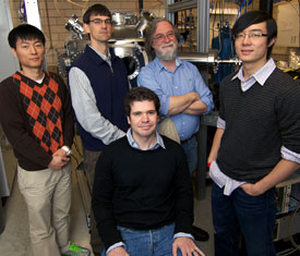 |
| (l to r) Young Il Joe, Peter Abbamonte, Eduardo Fradkin, Yu Gan; (seated) Bruno Uchoa. Photo by Hsin-Mao Wu |
Abstract:
Using advanced x-ray scattering techniques, physicists in Peter Abbamonte's group at the University of Illinois at Urbana-Champaign have imaged the motion of electrons in graphene with resolutions of 0.533 Ĺ and 10.3 attoseconds.
Ultrafast imaging of electron waves in graphene
Urbana, IL | Posted on December 8th, 2010The fastest movies ever made of electron motion, created by scattering x-rays off of graphene, have shown that the interaction among its electrons is surprisingly weak.
Graphene is a single atomic layer of carbon whose unusual electronic structure makes it a candidate for a new generation of low-cost, flexible electronics. A major outstanding question is whether the electrons in graphene move independently, or if their motion is correlated by Coulomb repulsion.
Using advanced x-ray scattering techniques, physicists in Peter Abbamonte's group at the University of Illinois at Urbana-Champaign have imaged the motion of electrons in graphene with resolutions of 0.533 Ĺ and 10.3 attoseconds. Their results were published on November 5 in Science.
Exactly how small and how fast are these measurements? An angstrom is 1/10,000,000,000 of a meter, about the width of a hydrogen atom. And an attosecond is to a second as a second is to the age of the universe.
The researchers found that graphene screens Coulomb interactions surprisingly effectively, causing it to act like a simple, independent-electron semimetal. Their work explains several mysteries, including why freestanding graphene fails to become an insulator as predicted. The study also demonstrates a new approach to studying ultrafast dynamics, creating a new window on the most fundamental properties of materials.
The experiments were carried out at the Frederick Seitz Materials Research Laboratory at the University of Illinois and the Advanced Photon Source at Argonne National Laboratory.
This work was supported by the U.S. Department of Energy under grants DE-FG02-07ER46459 and DE-FG02-07ER46453 through the Frederick Seitz Materials Research Laboratory, with use of the Advanced Photon Source supported by DEAC02- 06CH11357. The conclusions presented are those of the researchers and do not necessarily reflect the views of the U.S. Department of Energy.
####
For more information, please click here
Contacts:
Celia M. Elliott
217.244.7725
Copyright © University of Illinois at Urbana-Champaign
If you have a comment, please Contact us.Issuers of news releases, not 7th Wave, Inc. or Nanotechnology Now, are solely responsible for the accuracy of the content.
Bookmark:


| Related News Press |
News and information
![]() Simulating magnetization in a Heisenberg quantum spin chain April 5th, 2024
Simulating magnetization in a Heisenberg quantum spin chain April 5th, 2024
![]() NRL charters Navy’s quantum inertial navigation path to reduce drift April 5th, 2024
NRL charters Navy’s quantum inertial navigation path to reduce drift April 5th, 2024
![]() Discovery points path to flash-like memory for storing qubits: Rice find could hasten development of nonvolatile quantum memory April 5th, 2024
Discovery points path to flash-like memory for storing qubits: Rice find could hasten development of nonvolatile quantum memory April 5th, 2024
Videos/Movies
![]() New X-ray imaging technique to study the transient phases of quantum materials December 29th, 2022
New X-ray imaging technique to study the transient phases of quantum materials December 29th, 2022
![]() Solvent study solves solar cell durability puzzle: Rice-led project could make perovskite cells ready for prime time September 23rd, 2022
Solvent study solves solar cell durability puzzle: Rice-led project could make perovskite cells ready for prime time September 23rd, 2022
![]() Scientists prepare for the world’s smallest race: Nanocar Race II March 18th, 2022
Scientists prepare for the world’s smallest race: Nanocar Race II March 18th, 2022
![]() Visualizing the invisible: New fluorescent DNA label reveals nanoscopic cancer features March 4th, 2022
Visualizing the invisible: New fluorescent DNA label reveals nanoscopic cancer features March 4th, 2022
Govt.-Legislation/Regulation/Funding/Policy
![]() NRL charters Navy’s quantum inertial navigation path to reduce drift April 5th, 2024
NRL charters Navy’s quantum inertial navigation path to reduce drift April 5th, 2024
![]() Discovery points path to flash-like memory for storing qubits: Rice find could hasten development of nonvolatile quantum memory April 5th, 2024
Discovery points path to flash-like memory for storing qubits: Rice find could hasten development of nonvolatile quantum memory April 5th, 2024
![]() Chemical reactions can scramble quantum information as well as black holes April 5th, 2024
Chemical reactions can scramble quantum information as well as black holes April 5th, 2024
Academic/Education
![]() Rice University launches Rice Synthetic Biology Institute to improve lives January 12th, 2024
Rice University launches Rice Synthetic Biology Institute to improve lives January 12th, 2024
![]() Multi-institution, $4.6 million NSF grant to fund nanotechnology training September 9th, 2022
Multi-institution, $4.6 million NSF grant to fund nanotechnology training September 9th, 2022
Nanotubes/Buckyballs/Fullerenes/Nanorods/Nanostrings
![]() Tests find no free-standing nanotubes released from tire tread wear September 8th, 2023
Tests find no free-standing nanotubes released from tire tread wear September 8th, 2023
![]() Detection of bacteria and viruses with fluorescent nanotubes July 21st, 2023
Detection of bacteria and viruses with fluorescent nanotubes July 21st, 2023
Announcements
![]() NRL charters Navy’s quantum inertial navigation path to reduce drift April 5th, 2024
NRL charters Navy’s quantum inertial navigation path to reduce drift April 5th, 2024
![]() Discovery points path to flash-like memory for storing qubits: Rice find could hasten development of nonvolatile quantum memory April 5th, 2024
Discovery points path to flash-like memory for storing qubits: Rice find could hasten development of nonvolatile quantum memory April 5th, 2024
Tools
![]() Ferroelectrically modulate the Fermi level of graphene oxide to enhance SERS response November 3rd, 2023
Ferroelectrically modulate the Fermi level of graphene oxide to enhance SERS response November 3rd, 2023
![]() The USTC realizes In situ electron paramagnetic resonance spectroscopy using single nanodiamond sensors November 3rd, 2023
The USTC realizes In situ electron paramagnetic resonance spectroscopy using single nanodiamond sensors November 3rd, 2023
|
|
||
|
|
||
| The latest news from around the world, FREE | ||
|
|
||
|
|
||
| Premium Products | ||
|
|
||
|
Only the news you want to read!
Learn More |
||
|
|
||
|
Full-service, expert consulting
Learn More |
||
|
|
||