Home > Press > Shining light on a needle in a haystack
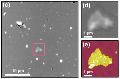 |
| "Laser targeting" for nanoscale microscopy: On the left, a typical 900 square micrometer view, using focused laser beam, shows potentially interesting purple membrane patch, which is marked with the square. Right top, closer optical image of patch; bottom, same target imaged with AFM revealing topological detail. Credit: A.B. Churnside, University of Colorado at Boulder |
Abstract:
In a new paper,* a group from JILA—a joint venture of the National Institute of Standards and Technology (NIST) and the University of Colorado—finds tiny assemblies of biomolecules for subsequent detailed imaging by combining precision laser optics with atomic force microscopy.
Shining light on a needle in a haystack
Gaithersburg, MD | Posted on November 10th, 2010The researchers characterize their new technique as a neat solution to the "needle in a haystack" problem of nanoscale microscopy, but it's more like the difference between finding the coffee table in a darkened room either by walking around until you fall over it, or using a flashlight.
The atomic force microscope (AFM) has become one of the standard tools of nanotechnology. The concept is deceptively simple. A needle—not unlike an old-fashioned phonograph stylus, but much smaller with a tip at most only a couple of atoms wide—moves across the surface of the specimen. A laser measures tiny deflections of the tip as it is pushed or pulled by atomic scale forces, such as electrostatic forces or chemical attraction. Scanning the tip back and forth across the sample yields a three-dimensional image of the surface. The resolution can be astonishing—in some cases showing individual atoms, a resolution a thousand times smaller than the best optical microscopes can achieve.
Such amazing sensitivity incurs a technical problem: if your probe can image an object of, say, 100 square nanometers, how exactly do you find that object if it could be nearly anywhere on a microscope stage a million times that size? That's not an unusual case in biological applications. The brute-force answer is, you scan the probe back and forth, probably at a higher speed, until it runs into something interesting. Like the coffee table in the dark, this has problems. The AFM tip is not only very delicate and easy to damage, but it can be degraded by picking up unwanted atoms or molecules from the surface. Also, in the biosciences, where the AFM is becoming increasingly important, research specimens usually are "soft" things like proteins or membranes that can be damaged by an uncontrolled collision with the tip. One solution has been to "label" the target molecule with a small fluorescent compound or quantum dot, so that it lights up and is easy to find, but that means chemically altering the subject, which may not be desirable.
Instead, the JILA team opted to use a flashlight. Building upon an earlier innovation for stabilizing the position of an AFM tip, the group uses a tightly focused, low-power laser beam to optically scan the area, identifying target locations by minute changes in the scattered light. This laser is scanned across the sample to form an image, analogous to forming an AFM image.
The same laser—and detection technique—is used to locate the AFM tip. Hence, the laser serves as a common frame of reference and it's relatively straightforward to align the optical and the AFM image. In experiments with patches of cell membrane from single-cell organisms,** the group has demonstrated that they can locate these protein complexes and align the AFM tip with a precision of about 40 nanometers. Relying solely on scattered light, their technique requires no prior chemical labeling or modification of the target molecules.
"You solve a couple of problems," says NIST physicist Thomas Perkins. "You solve the problem of finding the object you want to study, which is sort of a needle in a haystack problem. You solve the problem of not contaminating your tip. And, you solve the problem of not crashing your tip into what you were looking for. This prevents damaging your tip and, for soft biological targets, not damaging your sample." And, he says, it's much more efficient. "From a practical perspective, instead of my grad student starting to do real science at 4 p.m., she can start doing science at 10 a.m."
* A.B. Churnside, G.M. King and T.T. Perkins. Label-free optical imaging of membrane patches for atomic force microscopy. Optics Express. Vol. 18, No. 23. Nov. 8, 2010.
** The team used "purple membrane," which is cell membrane from certain single-cell organisms and contains bacteriorhodopsin, a protein that captures light energy. Bacteriorhodopsin is embedded in purple membrane and is a common protein for research in the biosciences.
####
For more information, please click here
Contacts:
Michael Baum
301-975-2763
National Institute of Standards and Technology (NIST)
Copyright © NIST
If you have a comment, please Contact us.Issuers of news releases, not 7th Wave, Inc. or Nanotechnology Now, are solely responsible for the accuracy of the content.
Bookmark:


| Related News Press |
News and information
![]() Simulating magnetization in a Heisenberg quantum spin chain April 5th, 2024
Simulating magnetization in a Heisenberg quantum spin chain April 5th, 2024
![]() NRL charters Navy’s quantum inertial navigation path to reduce drift April 5th, 2024
NRL charters Navy’s quantum inertial navigation path to reduce drift April 5th, 2024
![]() Discovery points path to flash-like memory for storing qubits: Rice find could hasten development of nonvolatile quantum memory April 5th, 2024
Discovery points path to flash-like memory for storing qubits: Rice find could hasten development of nonvolatile quantum memory April 5th, 2024
Announcements
![]() NRL charters Navy’s quantum inertial navigation path to reduce drift April 5th, 2024
NRL charters Navy’s quantum inertial navigation path to reduce drift April 5th, 2024
![]() Discovery points path to flash-like memory for storing qubits: Rice find could hasten development of nonvolatile quantum memory April 5th, 2024
Discovery points path to flash-like memory for storing qubits: Rice find could hasten development of nonvolatile quantum memory April 5th, 2024
Interviews/Book Reviews/Essays/Reports/Podcasts/Journals/White papers/Posters
![]() Simulating magnetization in a Heisenberg quantum spin chain April 5th, 2024
Simulating magnetization in a Heisenberg quantum spin chain April 5th, 2024
![]() Discovery points path to flash-like memory for storing qubits: Rice find could hasten development of nonvolatile quantum memory April 5th, 2024
Discovery points path to flash-like memory for storing qubits: Rice find could hasten development of nonvolatile quantum memory April 5th, 2024
Tools
![]() Ferroelectrically modulate the Fermi level of graphene oxide to enhance SERS response November 3rd, 2023
Ferroelectrically modulate the Fermi level of graphene oxide to enhance SERS response November 3rd, 2023
![]() The USTC realizes In situ electron paramagnetic resonance spectroscopy using single nanodiamond sensors November 3rd, 2023
The USTC realizes In situ electron paramagnetic resonance spectroscopy using single nanodiamond sensors November 3rd, 2023
Photonics/Optics/Lasers
![]() With VECSELs towards the quantum internet Fraunhofer: IAF achieves record output power with VECSEL for quantum frequency converters April 5th, 2024
With VECSELs towards the quantum internet Fraunhofer: IAF achieves record output power with VECSEL for quantum frequency converters April 5th, 2024
![]() Nanoscale CL thermometry with lanthanide-doped heavy-metal oxide in TEM March 8th, 2024
Nanoscale CL thermometry with lanthanide-doped heavy-metal oxide in TEM March 8th, 2024
![]() Optically trapped quantum droplets of light can bind together to form macroscopic complexes March 8th, 2024
Optically trapped quantum droplets of light can bind together to form macroscopic complexes March 8th, 2024
![]() HKUST researchers develop new integration technique for efficient coupling of III-V and silicon February 16th, 2024
HKUST researchers develop new integration technique for efficient coupling of III-V and silicon February 16th, 2024
|
|
||
|
|
||
| The latest news from around the world, FREE | ||
|
|
||
|
|
||
| Premium Products | ||
|
|
||
|
Only the news you want to read!
Learn More |
||
|
|
||
|
Full-service, expert consulting
Learn More |
||
|
|
||