Home > Press > Advance could change modern electronics
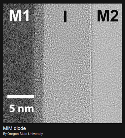 |
| This image of an asymmetric MIM diode reflects a major advance in materials science that could lead to less costly and higher speed electronic products. (Image courtesy of Oregon State University) |
Abstract:
Researchers at Oregon State University have solved a quest in fundamental material science that has eluded scientists since the 1960s, and could form the basis of a new approach to electronics.
Advance could change modern electronics
Corvallis, OR | Posted on October 30th, 2010The discovery, just reported online in the professional journal Advanced Materials, outlines the creation for the first time of a high-performance "metal-insulator-metal" diode.
"Researchers have been trying to do this for decades, until now without success," said Douglas Keszler, a distinguished professor of chemistry at OSU and one of the nation's leading material science researchers. "Diodes made previously with other approaches always had poor yield and performance.
"This is a fundamental change in the way you could produce electronic products, at high speed on a huge scale at very low cost, even less than with conventional methods," Keszler said. "It's a basic way to eliminate the current speed limitations of electrons that have to move through materials."
A patent has been applied for on the new technology, university officials say. New companies, industries and high-tech jobs may ultimately emerge from this advance, they say.
The research was done in the Center for Green Materials Chemistry, and has been supported by the National Science Foundation, the Army Research Laboratory and the Oregon Nanoscience and Microtechnologies Institute.
Conventional electronics made with silicon-based materials work with transistors that help control the flow of electrons. Although fast and comparatively inexpensive, this approach is still limited by the speed with which electrons can move through these materials. And with the advent of ever-faster computers and more sophisticated products such as liquid crystal displays, current technologies are nearing the limit of what they can do, experts say.
By contrast, a metal-insulator-metal, or MIM diode can be used to perform some of the same functions, but in a fundamentally different way. In this system, the device is like a sandwich, with the insulator in the middle and two layers of metal above and below it. In order to function, the electron doesn't so much move through the materials as it "tunnels" through the insulator - almost instantaneously appearing on the other side.
"When they first started to develop more sophisticated materials for the display industry, they knew this type of MIM diode was what they needed, but they couldn't make it work," Keszler said. "Now we can, and it could probably be used with a range of metals that are inexpensive and easily available, like copper, nickel or aluminum. It's also much simpler, less costly and easier to fabricate."
The findings were made by researchers in the OSU Department of Chemistry; School of Electrical Engineering and Computer Science; and School of Mechanical, Industrial and Manufacturing Engineering.
In the new study, the OSU scientists and engineers describe use of an "amorphous metal contact" as a technology that solves problems that previously plagued MIM diodes. The OSU diodes were made at relatively low temperatures with techniques that would lend themselves to manufacture of devices on a variety of substrates over large areas.
OSU researchers have been leaders in a number of important material science advances in recent years, including the field of transparent electronics. University scientists will do some initial work with the new technology in electronic displays, but many applications are possible, they say.
High speed computers and electronics that don't depend on transistors are possibilities. Also on the horizon are "energy harvesting" technologies such as the nighttime capture of re-radiated solar energy, a way to produce energy from the Earth as it cools during the night.
"For a long time, everyone has wanted something that takes us beyond silicon," Keszler said. "This could be a way to simply print electronics on a huge size scale even less expensively than we can now. And when the products begin to emerge the increase in speed of operation could be enormous."
####
About Oregon State University
OSU is one of only two U.S. universities designated a land-, sea-, space- and sun-grant institution. OSU is also Oregon�s only university designated in the Carnegie Foundation�s top tier for research institutions, garnering more than 60 percent of the total federal and private research funding in the Oregon University System. Its nearly 24,000 students come from all 50 states and more than 90 countries. OSU programs touch every county within Oregon, and its faculty teach and conduct research on issues of national and global importance.
For more information, please click here
Contacts:
Douglas Keszler
541-737-6736
John Wager
541-737-2994
John Conley
541-737-9874
Copyright © Oregon State University
If you have a comment, please Contact us.Issuers of news releases, not 7th Wave, Inc. or Nanotechnology Now, are solely responsible for the accuracy of the content.
Bookmark:


| Related News Press |
News and information
![]() Simulating magnetization in a Heisenberg quantum spin chain April 5th, 2024
Simulating magnetization in a Heisenberg quantum spin chain April 5th, 2024
![]() NRL charters Navy�s quantum inertial navigation path to reduce drift April 5th, 2024
NRL charters Navy�s quantum inertial navigation path to reduce drift April 5th, 2024
![]() Discovery points path to flash-like memory for storing qubits: Rice find could hasten development of nonvolatile quantum memory April 5th, 2024
Discovery points path to flash-like memory for storing qubits: Rice find could hasten development of nonvolatile quantum memory April 5th, 2024
Govt.-Legislation/Regulation/Funding/Policy
![]() NRL charters Navy�s quantum inertial navigation path to reduce drift April 5th, 2024
NRL charters Navy�s quantum inertial navigation path to reduce drift April 5th, 2024
![]() Discovery points path to flash-like memory for storing qubits: Rice find could hasten development of nonvolatile quantum memory April 5th, 2024
Discovery points path to flash-like memory for storing qubits: Rice find could hasten development of nonvolatile quantum memory April 5th, 2024
![]() Chemical reactions can scramble quantum information as well as black holes April 5th, 2024
Chemical reactions can scramble quantum information as well as black holes April 5th, 2024
Possible Futures
![]() Discovery points path to flash-like memory for storing qubits: Rice find could hasten development of nonvolatile quantum memory April 5th, 2024
Discovery points path to flash-like memory for storing qubits: Rice find could hasten development of nonvolatile quantum memory April 5th, 2024
![]() With VECSELs towards the quantum internet Fraunhofer: IAF achieves record output power with VECSEL for quantum frequency converters April 5th, 2024
With VECSELs towards the quantum internet Fraunhofer: IAF achieves record output power with VECSEL for quantum frequency converters April 5th, 2024
Academic/Education
![]() Rice University launches Rice Synthetic Biology Institute to improve lives January 12th, 2024
Rice University launches Rice Synthetic Biology Institute to improve lives January 12th, 2024
![]() Multi-institution, $4.6 million NSF grant to fund nanotechnology training September 9th, 2022
Multi-institution, $4.6 million NSF grant to fund nanotechnology training September 9th, 2022
Chip Technology
![]() Discovery points path to flash-like memory for storing qubits: Rice find could hasten development of nonvolatile quantum memory April 5th, 2024
Discovery points path to flash-like memory for storing qubits: Rice find could hasten development of nonvolatile quantum memory April 5th, 2024
![]() Utilizing palladium for addressing contact issues of buried oxide thin film transistors April 5th, 2024
Utilizing palladium for addressing contact issues of buried oxide thin film transistors April 5th, 2024
![]() HKUST researchers develop new integration technique for efficient coupling of III-V and silicon February 16th, 2024
HKUST researchers develop new integration technique for efficient coupling of III-V and silicon February 16th, 2024
Nanoelectronics
![]() Interdisciplinary: Rice team tackles the future of semiconductors Multiferroics could be the key to ultralow-energy computing October 6th, 2023
Interdisciplinary: Rice team tackles the future of semiconductors Multiferroics could be the key to ultralow-energy computing October 6th, 2023
![]() Key element for a scalable quantum computer: Physicists from Forschungszentrum J�lich and RWTH Aachen University demonstrate electron transport on a quantum chip September 23rd, 2022
Key element for a scalable quantum computer: Physicists from Forschungszentrum J�lich and RWTH Aachen University demonstrate electron transport on a quantum chip September 23rd, 2022
![]() Reduced power consumption in semiconductor devices September 23rd, 2022
Reduced power consumption in semiconductor devices September 23rd, 2022
![]() Atomic level deposition to extend Moore�s law and beyond July 15th, 2022
Atomic level deposition to extend Moore�s law and beyond July 15th, 2022
Discoveries
![]() Chemical reactions can scramble quantum information as well as black holes April 5th, 2024
Chemical reactions can scramble quantum information as well as black holes April 5th, 2024
![]() New micromaterial releases nanoparticles that selectively destroy cancer cells April 5th, 2024
New micromaterial releases nanoparticles that selectively destroy cancer cells April 5th, 2024
![]() Utilizing palladium for addressing contact issues of buried oxide thin film transistors April 5th, 2024
Utilizing palladium for addressing contact issues of buried oxide thin film transistors April 5th, 2024
Materials/Metamaterials/Magnetoresistance
![]() Nanoscale CL thermometry with lanthanide-doped heavy-metal oxide in TEM March 8th, 2024
Nanoscale CL thermometry with lanthanide-doped heavy-metal oxide in TEM March 8th, 2024
![]() Focused ion beam technology: A single tool for a wide range of applications January 12th, 2024
Focused ion beam technology: A single tool for a wide range of applications January 12th, 2024
Announcements
![]() NRL charters Navy�s quantum inertial navigation path to reduce drift April 5th, 2024
NRL charters Navy�s quantum inertial navigation path to reduce drift April 5th, 2024
![]() Discovery points path to flash-like memory for storing qubits: Rice find could hasten development of nonvolatile quantum memory April 5th, 2024
Discovery points path to flash-like memory for storing qubits: Rice find could hasten development of nonvolatile quantum memory April 5th, 2024
|
|
||
|
|
||
| The latest news from around the world, FREE | ||
|
|
||
|
|
||
| Premium Products | ||
|
|
||
|
Only the news you want to read!
Learn More |
||
|
|
||
|
Full-service, expert consulting
Learn More |
||
|
|
||