Home > Press > New Graphene Fabrication Method Uses Silicon Carbide Template
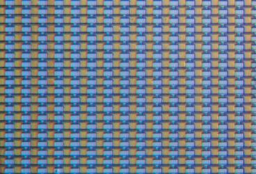 |
| Graphene transistors - Georgia Tech researchers have fabricated an array of 10,000 top-gated graphene transistors, believed to be the largest graphene device density reported so far. |
Abstract:
Researchers at the Georgia Institute of Technology have developed a new "templated growth" technique for fabricating nanometer-scale graphene devices. The method addresses what had been a significant obstacle to the use of this promising material in future generations of high-performance electronic devices.
New Graphene Fabrication Method Uses Silicon Carbide Template
Atlanta, GA | Posted on October 11th, 2010The technique involves etching patterns into the silicon carbide surfaces on which epitaxial graphene is grown. The patterns serve as templates directing the growth of graphene structures, allowing the formation of nanoribbons of specific widths without the use of e-beams or other destructive cutting techniques. Graphene nanoribbons produced with these templates have smooth edges that avoid electron-scattering problems.
"Using this approach, we can make very narrow ribbons of interconnected graphene without the rough edges," said Walt de Heer, a professor in the Georgia Tech School of Physics. "Anything that can be done to make small structures without having to cut them is going to be useful to the development of graphene electronics because if the edges are too rough, electrons passing through the ribbons scatter against the edges and reduce the desirable properties of graphene."
The new technique has been used to fabricate an array of 10,000 top-gated graphene transistors on a 0.24 square centimeter chip - believed to be the largest density of graphene devices reported so far.
The research was reported Oct. 3 in the advance online edition of the journal Nature Nanotechnology. The work was supported by the National Science Foundation, the W.M. Keck Foundation and the Nanoelectronics Research Initiative Institute for Nanoelectronics Discovery and Exploration (INDEX).
In creating their graphene nanostructures, De Heer and his research team first use conventional microelectronics techniques to etch tiny "steps" - or contours - into a silicon carbide wafer. They then heat the contoured wafer to approximately 1,500 degrees Celsius, which initiates melting that polishes any rough edges left by the etching process.
They then use established techniques for growing graphene from silicon carbide by driving off the silicon atoms from the surface. Instead of producing a consistent layer of graphene one atom thick across the surface of the wafer, however, the researchers limit the heating time so that graphene grows only on the edges of the contours.
To do this, they take advantage of the fact that graphene grows more rapidly on certain facets of the silicon carbide crystal than on others. The width of the resulting nanoribbons is proportional to the depth of the contour, providing a mechanism for precisely controlling the nanoribbons. To form complex graphene structures, multiple etching steps can be carried out to create a complex template, de Heer explained.
"By using the silicon carbide to provide the template, we can grow graphene in exactly the sizes and shapes that we want," he said. "Cutting steps of various depths allows us to create graphene structures that are interconnected in the way we want them to be."
In nanometer-scale graphene ribbons, quantum confinement makes the material behave as a semiconductor suitable for creation of electronic devices. But in ribbons a micron or more wide, the material acts as a conductor. Controlling the depth of the silicon carbide template allows the researchers to create these different structures simultaneously, using the same growth process.
"The same material can be either a conductor or a semiconductor depending on its shape," noted de Heer, who is also a faculty member in Georgia Tech's National Science Foundation-supported Materials Research Science and Engineering Center (MRSEC). "One of the major advantages of graphene electronics is to make the device leads and the semiconducting ribbons from the same material. That's important to avoid electrical resistance that builds up at junctions between different materials."
After formation of the nanoribbons - which can be as narrow as 40 nanometers - the researchers apply a dielectric material and metal gate to construct field-effect transistors. While successful fabrication of high-quality transistors demonstrates graphene's viability as an electronic material, de Heer sees them as only the first step in what could be done with the material.
"When we manage to make devices well on the nanoscale, we can then move on to make much smaller and finer structures that will go beyond conventional transistors to open up the possibility for more sophisticated devices that use electrons more like light than particles," he said. "If we can factor quantum mechanical features into electronics, that is going to open up a lot of new possibilities."
De Heer and his research team are now working to create smaller structures, and to integrate the graphene devices with silicon. The researchers are also working to improve the field-effect transistors with thinner dielectric materials.
Ultimately, graphene may be the basis for a generation of high-performance devices that will take advantage of the material's unique properties in applications where the higher cost can be justified. Silicon will continue to be used in applications that don't require such high performance, de Heer said.
"This is another step showing that our method of working with epitaxial graphene on silicon carbide is the right approach and the one that will probably be used for making graphene electronics," he added. "This is a significant new step toward electronics manufacturing with graphene."
In addition to those already mentioned, the research has involved M. Sprinkle, M. Ruan, Y Hu, J. Hankinson, M. Rubio-Roy, B. Zhang, X. Wu and C. Berger.
####
For more information, please click here
Contacts:
Media Relations Contacts:
John Toon
404-894-6986
Abby Vogel Robinson
404-385-3364
Copyright © Georgia Institute of Technology
If you have a comment, please Contact us.Issuers of news releases, not 7th Wave, Inc. or Nanotechnology Now, are solely responsible for the accuracy of the content.
Bookmark:


| Related News Press |
News and information
![]() Simulating magnetization in a Heisenberg quantum spin chain April 5th, 2024
Simulating magnetization in a Heisenberg quantum spin chain April 5th, 2024
![]() NRL charters Navy�s quantum inertial navigation path to reduce drift April 5th, 2024
NRL charters Navy�s quantum inertial navigation path to reduce drift April 5th, 2024
![]() Discovery points path to flash-like memory for storing qubits: Rice find could hasten development of nonvolatile quantum memory April 5th, 2024
Discovery points path to flash-like memory for storing qubits: Rice find could hasten development of nonvolatile quantum memory April 5th, 2024
Govt.-Legislation/Regulation/Funding/Policy
![]() NRL charters Navy�s quantum inertial navigation path to reduce drift April 5th, 2024
NRL charters Navy�s quantum inertial navigation path to reduce drift April 5th, 2024
![]() Discovery points path to flash-like memory for storing qubits: Rice find could hasten development of nonvolatile quantum memory April 5th, 2024
Discovery points path to flash-like memory for storing qubits: Rice find could hasten development of nonvolatile quantum memory April 5th, 2024
![]() Chemical reactions can scramble quantum information as well as black holes April 5th, 2024
Chemical reactions can scramble quantum information as well as black holes April 5th, 2024
Academic/Education
![]() Rice University launches Rice Synthetic Biology Institute to improve lives January 12th, 2024
Rice University launches Rice Synthetic Biology Institute to improve lives January 12th, 2024
![]() Multi-institution, $4.6 million NSF grant to fund nanotechnology training September 9th, 2022
Multi-institution, $4.6 million NSF grant to fund nanotechnology training September 9th, 2022
Chip Technology
![]() Discovery points path to flash-like memory for storing qubits: Rice find could hasten development of nonvolatile quantum memory April 5th, 2024
Discovery points path to flash-like memory for storing qubits: Rice find could hasten development of nonvolatile quantum memory April 5th, 2024
![]() Utilizing palladium for addressing contact issues of buried oxide thin film transistors April 5th, 2024
Utilizing palladium for addressing contact issues of buried oxide thin film transistors April 5th, 2024
![]() HKUST researchers develop new integration technique for efficient coupling of III-V and silicon February 16th, 2024
HKUST researchers develop new integration technique for efficient coupling of III-V and silicon February 16th, 2024
Nanoelectronics
![]() Interdisciplinary: Rice team tackles the future of semiconductors Multiferroics could be the key to ultralow-energy computing October 6th, 2023
Interdisciplinary: Rice team tackles the future of semiconductors Multiferroics could be the key to ultralow-energy computing October 6th, 2023
![]() Key element for a scalable quantum computer: Physicists from Forschungszentrum J�lich and RWTH Aachen University demonstrate electron transport on a quantum chip September 23rd, 2022
Key element for a scalable quantum computer: Physicists from Forschungszentrum J�lich and RWTH Aachen University demonstrate electron transport on a quantum chip September 23rd, 2022
![]() Reduced power consumption in semiconductor devices September 23rd, 2022
Reduced power consumption in semiconductor devices September 23rd, 2022
![]() Atomic level deposition to extend Moore�s law and beyond July 15th, 2022
Atomic level deposition to extend Moore�s law and beyond July 15th, 2022
Announcements
![]() NRL charters Navy�s quantum inertial navigation path to reduce drift April 5th, 2024
NRL charters Navy�s quantum inertial navigation path to reduce drift April 5th, 2024
![]() Discovery points path to flash-like memory for storing qubits: Rice find could hasten development of nonvolatile quantum memory April 5th, 2024
Discovery points path to flash-like memory for storing qubits: Rice find could hasten development of nonvolatile quantum memory April 5th, 2024
|
|
||
|
|
||
| The latest news from around the world, FREE | ||
|
|
||
|
|
||
| Premium Products | ||
|
|
||
|
Only the news you want to read!
Learn More |
||
|
|
||
|
Full-service, expert consulting
Learn More |
||
|
|
||