Home > Press > Researchers Develop Techniques for Using Material Recognized in Nobel Prize
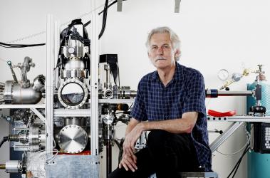 |
| Walt de Heer in laboratory - A team headed by Georgia Tech professor Walt de Heer has pioneered fabrication techniques for producing electronic devices from graphene. (Credit: Mali Azima) |
Abstract:
Georgia Institute of Technology researchers have pioneered the fabrication techniques expected to be used for manufacturing high-performance electronic devices from the material that has been recognized in this year's Nobel Prize in physics.
Researchers Develop Techniques for Using Material Recognized in Nobel Prize
Atlanta, GA | Posted on October 11th, 2010The 2010 physics prize was awarded for producing, isolating, identifying and characterizing graphene, a single atomic layer of carbon whose unique properties make the material attractive for electronic applications. Scientists at the University of Manchester were recognized for their work on graphene sheets peeled from blocks of graphite.
The work of the Georgia Tech group, headed by Professor Walt de Heer in the Georgia Tech School of Physics, was recognized by the Royal Swedish Academy of Sciences in its scientific background document on the physics prize. De Heer's group pioneered epitaxial techniques for growing large-scale graphene sheets by heating wafers of silicon carbide to drive off the silicon, leaving a thin layer of graphene.
The technique, which is now being used by research groups at companies such as IBM, has practical applications in large-scale production of electronic devices. On Oct. 3, the group published a paper in the journal Nature Nanotechnology describing a new technique used to produce an array of 10,000 graphene transistors.
"We believe that our technique, or one very much like it, will ultimately be used to manufacture future generations of graphene-based electronic devices," said de Heer. "Using techniques that are suitable for scaling up for mass production, we can grow graphene in the patterns that we need for electronic devices."
The Georgia Tech group holds a patent, filed in 2003, on fabricating electronic devices from these graphene layers.
Georgia Tech is home to a Materials Research Science and Engineering Center (MRSEC), funded by the National Science Foundation (NSF) and including collaborators from the University of California-Berkeley, University of California-Riverside and University of Michigan. The foundation focus of the center is research and development of epitaxial graphene.
"The unique properties of graphene portend considerable promise for future electronic and optical devices," said Dennis Hess, the center's director. "If graphene is to serve as a viable successor to silicon-based microelectronic devices and circuits, large scale production on a suitable substrate is required. Proof of concept of this approach has already been demonstrated by the fabrication of a 10,000 epitaxial graphene transistor array by Walt de Heer and his collaborators. This achievement is a significant advance toward realizing carbon-based electronics for the 21st century."
The Georgia Tech team also collaborates with researchers at the National Institute of Standards and Technology (NIST) on characterizing the unique properties of graphene. That work has led to several recent important papers, in journals such as Science and Nature Physics. The latter described for the first time how the orbits of electrons are distributed spatially by magnetic fields applied to layers of epitaxial graphene.
On Oct. 3 in the advance online publication of the journal Nature Nanotechnology, de Heer and collaborators described the development of a new "templated growth" technique for fabricating nanometer-scale graphene devices. The method addresses what had been a significant obstacle to the use of this promising material in future generations of high-performance electronic devices.
The technique involves etching patterns into the silicon carbide surfaces on which epitaxial graphene is grown. The patterns serve as templates directing the growth of graphene structures, allowing the formation of nanoribbons of specific widths without the use of e-beams or other destructive cutting techniques. Templated nanoribbon growth addresses the edge roughness that causes electron scattering.
####
For more information, please click here
Contacts:
Media Relations Contacts:
John Toon
404-894-6986
Abby Vogel Robinson
404-385-3364
Copyright © Georgia Institute of Technology
If you have a comment, please Contact us.Issuers of news releases, not 7th Wave, Inc. or Nanotechnology Now, are solely responsible for the accuracy of the content.
Bookmark:


| Related News Press |
News and information
![]() Simulating magnetization in a Heisenberg quantum spin chain April 5th, 2024
Simulating magnetization in a Heisenberg quantum spin chain April 5th, 2024
![]() NRL charters Navy�s quantum inertial navigation path to reduce drift April 5th, 2024
NRL charters Navy�s quantum inertial navigation path to reduce drift April 5th, 2024
![]() Discovery points path to flash-like memory for storing qubits: Rice find could hasten development of nonvolatile quantum memory April 5th, 2024
Discovery points path to flash-like memory for storing qubits: Rice find could hasten development of nonvolatile quantum memory April 5th, 2024
Possible Futures
![]() Discovery points path to flash-like memory for storing qubits: Rice find could hasten development of nonvolatile quantum memory April 5th, 2024
Discovery points path to flash-like memory for storing qubits: Rice find could hasten development of nonvolatile quantum memory April 5th, 2024
![]() With VECSELs towards the quantum internet Fraunhofer: IAF achieves record output power with VECSEL for quantum frequency converters April 5th, 2024
With VECSELs towards the quantum internet Fraunhofer: IAF achieves record output power with VECSEL for quantum frequency converters April 5th, 2024
Academic/Education
![]() Rice University launches Rice Synthetic Biology Institute to improve lives January 12th, 2024
Rice University launches Rice Synthetic Biology Institute to improve lives January 12th, 2024
![]() Multi-institution, $4.6 million NSF grant to fund nanotechnology training September 9th, 2022
Multi-institution, $4.6 million NSF grant to fund nanotechnology training September 9th, 2022
Chip Technology
![]() Discovery points path to flash-like memory for storing qubits: Rice find could hasten development of nonvolatile quantum memory April 5th, 2024
Discovery points path to flash-like memory for storing qubits: Rice find could hasten development of nonvolatile quantum memory April 5th, 2024
![]() Utilizing palladium for addressing contact issues of buried oxide thin film transistors April 5th, 2024
Utilizing palladium for addressing contact issues of buried oxide thin film transistors April 5th, 2024
![]() HKUST researchers develop new integration technique for efficient coupling of III-V and silicon February 16th, 2024
HKUST researchers develop new integration technique for efficient coupling of III-V and silicon February 16th, 2024
Nanotubes/Buckyballs/Fullerenes/Nanorods/Nanostrings
![]() Tests find no free-standing nanotubes released from tire tread wear September 8th, 2023
Tests find no free-standing nanotubes released from tire tread wear September 8th, 2023
![]() Detection of bacteria and viruses with fluorescent nanotubes July 21st, 2023
Detection of bacteria and viruses with fluorescent nanotubes July 21st, 2023
Nanoelectronics
![]() Interdisciplinary: Rice team tackles the future of semiconductors Multiferroics could be the key to ultralow-energy computing October 6th, 2023
Interdisciplinary: Rice team tackles the future of semiconductors Multiferroics could be the key to ultralow-energy computing October 6th, 2023
![]() Key element for a scalable quantum computer: Physicists from Forschungszentrum J�lich and RWTH Aachen University demonstrate electron transport on a quantum chip September 23rd, 2022
Key element for a scalable quantum computer: Physicists from Forschungszentrum J�lich and RWTH Aachen University demonstrate electron transport on a quantum chip September 23rd, 2022
![]() Reduced power consumption in semiconductor devices September 23rd, 2022
Reduced power consumption in semiconductor devices September 23rd, 2022
![]() Atomic level deposition to extend Moore�s law and beyond July 15th, 2022
Atomic level deposition to extend Moore�s law and beyond July 15th, 2022
Announcements
![]() NRL charters Navy�s quantum inertial navigation path to reduce drift April 5th, 2024
NRL charters Navy�s quantum inertial navigation path to reduce drift April 5th, 2024
![]() Discovery points path to flash-like memory for storing qubits: Rice find could hasten development of nonvolatile quantum memory April 5th, 2024
Discovery points path to flash-like memory for storing qubits: Rice find could hasten development of nonvolatile quantum memory April 5th, 2024
Patents/IP/Tech Transfer/Licensing
![]() Getting drugs across the blood-brain barrier using nanoparticles March 3rd, 2023
Getting drugs across the blood-brain barrier using nanoparticles March 3rd, 2023
![]() Metasurfaces control polarized light at will: New research unlocks the hidden potential of metasurfaces August 13th, 2021
Metasurfaces control polarized light at will: New research unlocks the hidden potential of metasurfaces August 13th, 2021
![]() Arrowhead Pharmaceuticals Announces Closing of Agreement with Takeda November 27th, 2020
Arrowhead Pharmaceuticals Announces Closing of Agreement with Takeda November 27th, 2020
Grants/Sponsored Research/Awards/Scholarships/Gifts/Contests/Honors/Records
![]() Discovery points path to flash-like memory for storing qubits: Rice find could hasten development of nonvolatile quantum memory April 5th, 2024
Discovery points path to flash-like memory for storing qubits: Rice find could hasten development of nonvolatile quantum memory April 5th, 2024
![]() Chemical reactions can scramble quantum information as well as black holes April 5th, 2024
Chemical reactions can scramble quantum information as well as black holes April 5th, 2024
Research partnerships
![]() Discovery points path to flash-like memory for storing qubits: Rice find could hasten development of nonvolatile quantum memory April 5th, 2024
Discovery points path to flash-like memory for storing qubits: Rice find could hasten development of nonvolatile quantum memory April 5th, 2024
![]() Researchers� approach may protect quantum computers from attacks March 8th, 2024
Researchers� approach may protect quantum computers from attacks March 8th, 2024
![]() 'Sudden death' of quantum fluctuations defies current theories of superconductivity: Study challenges the conventional wisdom of superconducting quantum transitions January 12th, 2024
'Sudden death' of quantum fluctuations defies current theories of superconductivity: Study challenges the conventional wisdom of superconducting quantum transitions January 12th, 2024
|
|
||
|
|
||
| The latest news from around the world, FREE | ||
|
|
||
|
|
||
| Premium Products | ||
|
|
||
|
Only the news you want to read!
Learn More |
||
|
|
||
|
Full-service, expert consulting
Learn More |
||
|
|
||