Home > Press > Stevens Institute of Technology Awarded NSF Grant
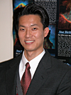 |
| Dr. Eui-Hyeok Yang |
Abstract:
Nanoimprint Lithography NSF Grant Awarded To Micro Device Lab At Stevens
Stevens Institute of Technology Awarded NSF Grant
Hoboken, NJ | Posted on October 11th, 2010Dr. Eu-Hyeok (EH)Yang, Associate Professor of Mechanical Engineering and Director of the Micro Device Laboratory (MDL) at Stevens Institute of Technology, The Innovation UniversityTM, will receive funding from the National Science Foundation (NSF) for the acquisition of a Nanoimprint Lithography System (NIL) for the purpose of nanoscience research and education based on low-dimensional materials at Stevens. The Co-PIs of the project are Drs. Besser, Choi, Cappelleri and Strauf. This equipment acquisition is an important step in achieving Dr. Yang's goal of integrating research and education in nanotechnology at the MDL. In addition, nanoimprint lithography will benefit local institutions searching for nearby solutions for nanopatterning. "The system will be an open local resource for researchers," Yang says.
"The NIL system is the latest piece of equipment in completing the fabrication process flow for micro/nano devices at Stevens," Yang says. "The MDL's capabilities for research and education increase significantly with this system."
The grant funds the acquisition of a Nanonex 1000 Nanoimprint Lithography System, a whole-wafer (4-inch) nanoimprinter for thermoplastic resins that has high-resolution (~10 nm) and high-throughput (~60 sec) capabilities. This acquisition will strengthen the exploration of high-throughput nanoscale patterning as a key part of the research projects funded by NSF, DARPA, US Army, AFOSR, and ONR. These inter-disciplinary, high-risk, high-payoff research projects will provide a consistently growing user base and cultivate a multidisciplinary research-intense learning environment in nanotechnology at Stevens along with collaborators in the New York City metropolitan area.
This research capability also supports cross-disciplinary educational initiatives already underway at Stevens. It provides hands-on experience to students in the Nanotechnology Graduate Program and undergraduates alike. One of Yang's undergraduate senior design teams plans to create an Intra Ocular Pressure Relief Valve, used to treat glaucoma by releasing fluid when pressure builds up in the eye. The nanoimprint lithography system will greatly benefit their fabrication process.
"The MDL is an integral component of the Nanotechnology research thrust at Stevens," says Michael Bruno, Dean of the Charles. V. Schaefer School of Engineering and Science. "The NIL acquisition enhances Stevens' capabilities for nanotechnology research in the area and simultaneously offers outside organizations a solution for their nanotechnology research needs."
Researchers at Stevens previously relied on an external nanoimprint lithography facility at the Center for Functional Nanomaterials (CFN) at the Brookhaven National Laboratory in Upton, NY. Therefore, the aavailability of the in-house nanoimprint lithography system will significantly increase the efficiency and output of work done in the laboratory, increase the training capabilities for Stevens staff and students, and enable many undergraduate and graduate educational initiatives. Investigators from and outside of Stevens will have easy access to nanoimprint lithography in the Micro Device Laboratory on the Stevens campus. Professor Ioana Voiculescu at City College of New York is listed as Senior Personnel of the Project.
"Over the next few years we will be a major force in nanotechnology research as this facility, along with future acquisitions, continues to grow," says Dr. Constantin Chassapis, Professor, Deputy Dean of the School of Engineering & Science, and Director of the Department of Mechanical Engineering.
####
For more information, please click here
Copyright © Stevens Institute of Technology
If you have a comment, please Contact us.Issuers of news releases, not 7th Wave, Inc. or Nanotechnology Now, are solely responsible for the accuracy of the content.
Bookmark:


| Related News Press |
News and information
![]() Simulating magnetization in a Heisenberg quantum spin chain April 5th, 2024
Simulating magnetization in a Heisenberg quantum spin chain April 5th, 2024
![]() NRL charters Navy�s quantum inertial navigation path to reduce drift April 5th, 2024
NRL charters Navy�s quantum inertial navigation path to reduce drift April 5th, 2024
![]() Discovery points path to flash-like memory for storing qubits: Rice find could hasten development of nonvolatile quantum memory April 5th, 2024
Discovery points path to flash-like memory for storing qubits: Rice find could hasten development of nonvolatile quantum memory April 5th, 2024
Chip Technology
![]() Discovery points path to flash-like memory for storing qubits: Rice find could hasten development of nonvolatile quantum memory April 5th, 2024
Discovery points path to flash-like memory for storing qubits: Rice find could hasten development of nonvolatile quantum memory April 5th, 2024
![]() Utilizing palladium for addressing contact issues of buried oxide thin film transistors April 5th, 2024
Utilizing palladium for addressing contact issues of buried oxide thin film transistors April 5th, 2024
![]() HKUST researchers develop new integration technique for efficient coupling of III-V and silicon February 16th, 2024
HKUST researchers develop new integration technique for efficient coupling of III-V and silicon February 16th, 2024
Nanoelectronics
![]() Interdisciplinary: Rice team tackles the future of semiconductors Multiferroics could be the key to ultralow-energy computing October 6th, 2023
Interdisciplinary: Rice team tackles the future of semiconductors Multiferroics could be the key to ultralow-energy computing October 6th, 2023
![]() Key element for a scalable quantum computer: Physicists from Forschungszentrum J�lich and RWTH Aachen University demonstrate electron transport on a quantum chip September 23rd, 2022
Key element for a scalable quantum computer: Physicists from Forschungszentrum J�lich and RWTH Aachen University demonstrate electron transport on a quantum chip September 23rd, 2022
![]() Reduced power consumption in semiconductor devices September 23rd, 2022
Reduced power consumption in semiconductor devices September 23rd, 2022
![]() Atomic level deposition to extend Moore�s law and beyond July 15th, 2022
Atomic level deposition to extend Moore�s law and beyond July 15th, 2022
Announcements
![]() NRL charters Navy�s quantum inertial navigation path to reduce drift April 5th, 2024
NRL charters Navy�s quantum inertial navigation path to reduce drift April 5th, 2024
![]() Discovery points path to flash-like memory for storing qubits: Rice find could hasten development of nonvolatile quantum memory April 5th, 2024
Discovery points path to flash-like memory for storing qubits: Rice find could hasten development of nonvolatile quantum memory April 5th, 2024
Tools
![]() Ferroelectrically modulate the Fermi level of graphene oxide to enhance SERS response November 3rd, 2023
Ferroelectrically modulate the Fermi level of graphene oxide to enhance SERS response November 3rd, 2023
![]() The USTC realizes In situ electron paramagnetic resonance spectroscopy using single nanodiamond sensors November 3rd, 2023
The USTC realizes In situ electron paramagnetic resonance spectroscopy using single nanodiamond sensors November 3rd, 2023
Grants/Sponsored Research/Awards/Scholarships/Gifts/Contests/Honors/Records
![]() Discovery points path to flash-like memory for storing qubits: Rice find could hasten development of nonvolatile quantum memory April 5th, 2024
Discovery points path to flash-like memory for storing qubits: Rice find could hasten development of nonvolatile quantum memory April 5th, 2024
![]() Chemical reactions can scramble quantum information as well as black holes April 5th, 2024
Chemical reactions can scramble quantum information as well as black holes April 5th, 2024
|
|
||
|
|
||
| The latest news from around the world, FREE | ||
|
|
||
|
|
||
| Premium Products | ||
|
|
||
|
Only the news you want to read!
Learn More |
||
|
|
||
|
Full-service, expert consulting
Learn More |
||
|
|
||