Home > Press > Student’s Discovery Advances Nanotech Research
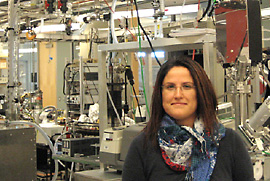 |
| Materials science graduate student Muge Acik has been working with graphene, a single sheet of carbon that exhibits unique electronic and mechanical properties. |
Abstract:
Enhanced, Ultra-Thin Sheets of Carbon Hold Promise in Sensor Applications
Student’s Discovery Advances Nanotech Research
Richardson, TX | Posted on October 7th, 2010A UT Dallas graduate student's surprising research results could ultimately lead to high-performance nanoelectronics applications such as electron emitters, thermal-infrared night-vision sensors and solar absorbers for harvesting sunlight.
Materials science graduate student Muge Acik has been working with graphene, a single sheet of carbon that exhibits unique electronic and mechanical properties, making it a candidate to eventually replace silicon in applications like ultrafast transistors.
Making real-world devices from graphene, however, depends upon controlling the edges of graphene sheets, which often dictate the material's electronic properties. Simply adding oxygen atoms at the edges may turn graphene into an insulator.
Performing her experimental work on graphene oxide (GO) in Dr. Yves Chabal's Laboratory for Surface and Nanostructure Modification, Acik discovered a new infrared absorption mechanism when GO is annealed to about 850°C to remove most oxygen. The result was a very special arrangement of oxygen atoms at the edges. This stable configuration fosters the electronic conduction or emission necessary for device operation and for electron emitters.
Moreover, "this new phenomenon opens the door to tailoring giant infrared absorption at different spectral positions by modifying the nature of the edge termination," she and her co-investigators concluded. And that opens the door to employing graphene in a number of nanoelectronic applications in which infrared absorption is important, such as night-vision sensors and sunlight-harvesting solar absorbers.
"This work is a good example where the contribution from theory has been critical, as provided by Dr. G. Lee, a postdoctoral fellow working under the supervision of Dr. Kyeongjae ‘KJ' Cho," said Chabal, head of materials science and engineering and holder of the Texas Instruments Distinguished University Chair in Nanoelectronics. "The theory provided a detailed understanding of this new phenomenon that would have remained puzzling on its own."
Cho added that "this experimental finding is consistent with an earlier theoretical prediction of the metallic state of graphene edge oxide published in Physical Review in 2009."
The team's results recently appeared in the journal Nature Materials in an article titled "Unusual Infrared Absorption Mechanism in Thermally Reduced Graphene Oxide."
This absorption is a new phenomenon that's unique to graphene, according to Chabal in an article that appeared in nanotechweb.org, noting that the potential applications are very exciting.
"The effect cannot be explained by simple infrared absorption mechanisms and can only happen if free, mobile electrons are induced in reduced graphene oxide - something that has never been observed before," the article concluded.
The research was funded by the Semiconductor Research Corp.'s Nanotechnology Research Initiative and by Texas Instruments. The work was done in collaboration with Cecilia Mattevi and Manish Chhowalla at Rutgers University. A synopsis of the Nature Materials article is featured under Nano Focus here.
####
For more information, please click here
Contacts:
Media Contact: David Moore, UT Dallas, (972) 883-4183,
Office of Media Relations, UT Dallas, (972) 883-2155,
Copyright © University of Texas at Dallas
If you have a comment, please Contact us.Issuers of news releases, not 7th Wave, Inc. or Nanotechnology Now, are solely responsible for the accuracy of the content.
Bookmark:


| Related News Press |
News and information
![]() Simulating magnetization in a Heisenberg quantum spin chain April 5th, 2024
Simulating magnetization in a Heisenberg quantum spin chain April 5th, 2024
![]() NRL charters Navy’s quantum inertial navigation path to reduce drift April 5th, 2024
NRL charters Navy’s quantum inertial navigation path to reduce drift April 5th, 2024
![]() Discovery points path to flash-like memory for storing qubits: Rice find could hasten development of nonvolatile quantum memory April 5th, 2024
Discovery points path to flash-like memory for storing qubits: Rice find could hasten development of nonvolatile quantum memory April 5th, 2024
Possible Futures
![]() Discovery points path to flash-like memory for storing qubits: Rice find could hasten development of nonvolatile quantum memory April 5th, 2024
Discovery points path to flash-like memory for storing qubits: Rice find could hasten development of nonvolatile quantum memory April 5th, 2024
![]() With VECSELs towards the quantum internet Fraunhofer: IAF achieves record output power with VECSEL for quantum frequency converters April 5th, 2024
With VECSELs towards the quantum internet Fraunhofer: IAF achieves record output power with VECSEL for quantum frequency converters April 5th, 2024
Academic/Education
![]() Rice University launches Rice Synthetic Biology Institute to improve lives January 12th, 2024
Rice University launches Rice Synthetic Biology Institute to improve lives January 12th, 2024
![]() Multi-institution, $4.6 million NSF grant to fund nanotechnology training September 9th, 2022
Multi-institution, $4.6 million NSF grant to fund nanotechnology training September 9th, 2022
Chip Technology
![]() Discovery points path to flash-like memory for storing qubits: Rice find could hasten development of nonvolatile quantum memory April 5th, 2024
Discovery points path to flash-like memory for storing qubits: Rice find could hasten development of nonvolatile quantum memory April 5th, 2024
![]() Utilizing palladium for addressing contact issues of buried oxide thin film transistors April 5th, 2024
Utilizing palladium for addressing contact issues of buried oxide thin film transistors April 5th, 2024
![]() HKUST researchers develop new integration technique for efficient coupling of III-V and silicon February 16th, 2024
HKUST researchers develop new integration technique for efficient coupling of III-V and silicon February 16th, 2024
Sensors
Nanoelectronics
![]() Interdisciplinary: Rice team tackles the future of semiconductors Multiferroics could be the key to ultralow-energy computing October 6th, 2023
Interdisciplinary: Rice team tackles the future of semiconductors Multiferroics could be the key to ultralow-energy computing October 6th, 2023
![]() Key element for a scalable quantum computer: Physicists from Forschungszentrum Jülich and RWTH Aachen University demonstrate electron transport on a quantum chip September 23rd, 2022
Key element for a scalable quantum computer: Physicists from Forschungszentrum Jülich and RWTH Aachen University demonstrate electron transport on a quantum chip September 23rd, 2022
![]() Reduced power consumption in semiconductor devices September 23rd, 2022
Reduced power consumption in semiconductor devices September 23rd, 2022
![]() Atomic level deposition to extend Moore’s law and beyond July 15th, 2022
Atomic level deposition to extend Moore’s law and beyond July 15th, 2022
Discoveries
![]() Chemical reactions can scramble quantum information as well as black holes April 5th, 2024
Chemical reactions can scramble quantum information as well as black holes April 5th, 2024
![]() New micromaterial releases nanoparticles that selectively destroy cancer cells April 5th, 2024
New micromaterial releases nanoparticles that selectively destroy cancer cells April 5th, 2024
![]() Utilizing palladium for addressing contact issues of buried oxide thin film transistors April 5th, 2024
Utilizing palladium for addressing contact issues of buried oxide thin film transistors April 5th, 2024
Announcements
![]() NRL charters Navy’s quantum inertial navigation path to reduce drift April 5th, 2024
NRL charters Navy’s quantum inertial navigation path to reduce drift April 5th, 2024
![]() Discovery points path to flash-like memory for storing qubits: Rice find could hasten development of nonvolatile quantum memory April 5th, 2024
Discovery points path to flash-like memory for storing qubits: Rice find could hasten development of nonvolatile quantum memory April 5th, 2024
Energy
![]() Development of zinc oxide nanopagoda array photoelectrode: photoelectrochemical water-splitting hydrogen production January 12th, 2024
Development of zinc oxide nanopagoda array photoelectrode: photoelectrochemical water-splitting hydrogen production January 12th, 2024
![]() Shedding light on unique conduction mechanisms in a new type of perovskite oxide November 17th, 2023
Shedding light on unique conduction mechanisms in a new type of perovskite oxide November 17th, 2023
![]() Inverted perovskite solar cell breaks 25% efficiency record: Researchers improve cell efficiency using a combination of molecules to address different November 17th, 2023
Inverted perovskite solar cell breaks 25% efficiency record: Researchers improve cell efficiency using a combination of molecules to address different November 17th, 2023
![]() The efficient perovskite cells with a structured anti-reflective layer – another step towards commercialization on a wider scale October 6th, 2023
The efficient perovskite cells with a structured anti-reflective layer – another step towards commercialization on a wider scale October 6th, 2023
Solar/Photovoltaic
![]() Development of zinc oxide nanopagoda array photoelectrode: photoelectrochemical water-splitting hydrogen production January 12th, 2024
Development of zinc oxide nanopagoda array photoelectrode: photoelectrochemical water-splitting hydrogen production January 12th, 2024
![]() Shedding light on unique conduction mechanisms in a new type of perovskite oxide November 17th, 2023
Shedding light on unique conduction mechanisms in a new type of perovskite oxide November 17th, 2023
![]() Inverted perovskite solar cell breaks 25% efficiency record: Researchers improve cell efficiency using a combination of molecules to address different November 17th, 2023
Inverted perovskite solar cell breaks 25% efficiency record: Researchers improve cell efficiency using a combination of molecules to address different November 17th, 2023
![]() Charged “molecular beasts” the basis for new compounds: Researchers at Leipzig University use “aggressive” fragments of molecular ions for chemical synthesis November 3rd, 2023
Charged “molecular beasts” the basis for new compounds: Researchers at Leipzig University use “aggressive” fragments of molecular ions for chemical synthesis November 3rd, 2023
|
|
||
|
|
||
| The latest news from around the world, FREE | ||
|
|
||
|
|
||
| Premium Products | ||
|
|
||
|
Only the news you want to read!
Learn More |
||
|
|
||
|
Full-service, expert consulting
Learn More |
||
|
|
||