Home > Press > Multi-touch Interface Creates New Electron Microscope Experience with JEOL InTouchScopeTM JEOL puts SEM “Apps” at your fingertips
 |
Abstract:
JEOL offers a whole new electron microscope experience with the introduction of the InTouchScopeTM, an analytical, low vacuum Scanning Electron Microscope (SEM) featuring integrated Energy Dispersive Spectroscopy (EDS) with the latest Silicon Drift Detector (SDD) technology.
Multi-touch Interface Creates New Electron Microscope Experience with JEOL InTouchScopeTM JEOL puts SEM “Apps” at your fingertips
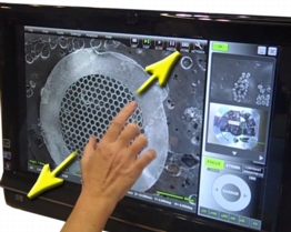
Peabody, MA | Posted on September 22nd, 2010The new InTouchScope has the familiar feel of today's personal electronic media. The intuitive multi-touch screen interface puts all SEM "Apps" at the operator's fingertips. The user can expand windows and images with the sweep of two fingers, dial in magnification and focus with a swipe, and select operating parameters, analytical functions, or measure distances just by tapping the PC or notebook touch screen.
Ease of use is a key feature of all JEOL SEMs, and the versatile InTouchScope has functions that users of all levels will appreciate:
* automatic SEM condition setup based on sample type
* simultaneous multiple live image and movie capture
* easy sample navigation at 5x - 300,000x magnifications
* quantitative and qualitative elemental analysis
* low and high vacuum operation
* wireless capability
The InTouchScope features all the capabilities of a full size tungsten SEM with integrated EDS analysis in a small, ergonomic and intuitive design. An onboard turbo pump make this a truly self-contained, portable SEM that is easy to set up anywhere in the lab.
####
About JEOL USA, Inc.
JEOL is a world leader in electron optical equipment and instrumentation for high-end scientific and industrial research and development. Core product groups include electron microscopes (SEMs and TEMs), instruments for the semiconductor industry (electron beam lithography and a series of defect review and inspection tools), and analytical instruments including mass spectrometers, NMRs and ESRs.
JEOL USA, Inc., a wholly owned subsidiary of JEOL, Ltd., Japan, was incorporated in the United States in 1962. The company has 13 regional service centers that offer unlimited emergency service and support in the U.S.
For more information, please click here
Contacts:
JEOL USA, Inc.
11 Dearborn Road
Peabody, MA 01960
978-535-5900
www.jeolusa.com
Press Contact:
Patricia Corkum
978-536-2273
Pamela Mansfield
JEOL USA
11 Dearborn Road
Peabody, MA 01960
978-536-2309
Copyright © JEOL USA, Inc.
If you have a comment, please Contact us.Issuers of news releases, not 7th Wave, Inc. or Nanotechnology Now, are solely responsible for the accuracy of the content.
Bookmark:


| Related News Press |
News and information
![]() Simulating magnetization in a Heisenberg quantum spin chain April 5th, 2024
Simulating magnetization in a Heisenberg quantum spin chain April 5th, 2024
![]() NRL charters Navy’s quantum inertial navigation path to reduce drift April 5th, 2024
NRL charters Navy’s quantum inertial navigation path to reduce drift April 5th, 2024
![]() Discovery points path to flash-like memory for storing qubits: Rice find could hasten development of nonvolatile quantum memory April 5th, 2024
Discovery points path to flash-like memory for storing qubits: Rice find could hasten development of nonvolatile quantum memory April 5th, 2024
Imaging
![]() Nanoscale CL thermometry with lanthanide-doped heavy-metal oxide in TEM March 8th, 2024
Nanoscale CL thermometry with lanthanide-doped heavy-metal oxide in TEM March 8th, 2024
![]() The USTC realizes In situ electron paramagnetic resonance spectroscopy using single nanodiamond sensors November 3rd, 2023
The USTC realizes In situ electron paramagnetic resonance spectroscopy using single nanodiamond sensors November 3rd, 2023
![]() Observation of left and right at nanoscale with optical force October 6th, 2023
Observation of left and right at nanoscale with optical force October 6th, 2023
Announcements
![]() NRL charters Navy’s quantum inertial navigation path to reduce drift April 5th, 2024
NRL charters Navy’s quantum inertial navigation path to reduce drift April 5th, 2024
![]() Discovery points path to flash-like memory for storing qubits: Rice find could hasten development of nonvolatile quantum memory April 5th, 2024
Discovery points path to flash-like memory for storing qubits: Rice find could hasten development of nonvolatile quantum memory April 5th, 2024
Tools
![]() Ferroelectrically modulate the Fermi level of graphene oxide to enhance SERS response November 3rd, 2023
Ferroelectrically modulate the Fermi level of graphene oxide to enhance SERS response November 3rd, 2023
![]() The USTC realizes In situ electron paramagnetic resonance spectroscopy using single nanodiamond sensors November 3rd, 2023
The USTC realizes In situ electron paramagnetic resonance spectroscopy using single nanodiamond sensors November 3rd, 2023
|
|
||
|
|
||
| The latest news from around the world, FREE | ||
|
|
||
|
|
||
| Premium Products | ||
|
|
||
|
Only the news you want to read!
Learn More |
||
|
|
||
|
Full-service, expert consulting
Learn More |
||
|
|
||