Home > Press > Engineers make artificial skin out of nanowires
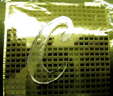 |
| Photo of an artificial skin made of nanowires. The e-skin was able to accurately sense the shape of the Cal "C" placed on top. |
Abstract:
Engineers at the University of California, Berkeley, have developed a pressure-sensitive electronic material from semiconductor nanowires that could one day give new meaning to the term "thin-skinned."
Engineers make artificial skin out of nanowires
Berkeley, CA | Posted on September 12th, 2010"The idea is to have a material that functions like the human skin, which means incorporating the ability to feel and touch objects," said Ali Javey, associate professor of electrical engineering and computer sciences and head of the UC Berkeley research team developing the artificial skin.
The artificial skin, dubbed "e-skin" by the UC Berkeley researchers, is described in a Sept. 12 paper in the advanced online publication of the journal Nature Materials. It is the first such material made out of inorganic single crystalline semiconductors.
A touch-sensitive artificial skin would help overcome a key challenge in robotics: adapting the amount of force needed to hold and manipulate a wide range of objects.
"Humans generally know how to hold a fragile egg without breaking it," said Javey, who is also a member of the Berkeley Sensor and Actuator Center and a faculty scientist at the Lawrence Berkeley National Laboratory Materials Sciences Division. "If we ever wanted a robot that could unload the dishes, for instance, we'd want to make sure it doesn't break the wine glasses in the process. But we'd also want the robot to be able to grip a stock pot without dropping it."
A longer term goal would be to use the e-skin to restore the sense of touch to patients with prosthetic limbs, which would require significant advances in the integration of electronic sensors with the human nervous system.
Previous attempts to develop an artificial skin relied upon organic materials because they are flexible and easier to process.
"The problem is that organic materials are poor semiconductors, which means electronic devices made out of them would often require high voltages to operate the circuitry," said Javey. "Inorganic materials, such as crystalline silicon, on the other hand, have excellent electrical properties and can operate on low power. They are also more chemically stable. But historically, they have been inflexible and easy to crack. In this regard, works by various groups, including ours, have recently shown that miniaturized strips or wires of inorganics can be made highly flexible � ideal for high performance, mechanically bendable electronics and sensors."
The UC Berkeley engineers utilized an innovative fabrication technique that works somewhat like a lint roller in reverse. Instead of picking up fibers, nanowire "hairs" are deposited.
The researchers started by growing the germanium/silicon nanowires on a cylindrical drum, which was then rolled onto a sticky substrate. The substrate used was a polyimide film, but the researchers said the technique can work with a variety of materials, including other plastics, paper or glass. As the drum rolled, the nanowires were deposited, or "printed," onto the substrate in an orderly fashion, forming the basis from which thin, flexible sheets of electronic materials could be built.
In another complementary approach utilized by the researchers, the nanowires were first grown on a flat source substrate, and then transferred to the polyimide film by a direction-rubbing process.
For the e-skin, the engineers printed the nanowires onto an 18-by-19 pixel square matrix measuring 7 centimeters on each side. Each pixel contained a transistor made up of hundreds of semiconductor nanowires. Nanowire transistors were then integrated with a pressure sensitive rubber on top to provide the sensing functionality. The matrix required less than 5 volts of power to operate and maintained its robustness after being subjected to more than 2,000 bending cycles.
The researchers demonstrated the ability of the e-skin to detect pressure from 0 to 15 kilopascals, a range comparable to the force used for such daily activities as typing on a keyboard or holding an object. In a nod to their home institution, the researchers successfully mapped out the letter C in Cal.
"This is the first truly macroscale integration of ordered nanowire materials for a functional system � in this case, an electronic skin," said study lead author Kuniharu Takei, post-doctoral fellow in electrical engineering and computer sciences. "It's a technique that can be potentially scaled up. The limit now to the size of the e-skin we developed is the size of the processing tools we are using."
Other UC Berkeley co-authors of the paper are Ron Fearing, professor of electrical engineering and computer sciences; Toshitake Takahashi, graduate student in electrical engineering and computer sciences; Johnny C. Ho, graduate student in materials science and engineering; Hyunhyub Ko and Paul Leu, post-doctoral researchers in electrical engineering and computer sciences; and Andrew G. Gillies, graduate student in mechanical engineering.
The National Science Foundation and the Defense Advanced Research Projects Agency helped support this research.
####
For more information, please click here
Contacts:
Ali Javey
(510) 643-7263
Kuniharu Takei
(510) 643-1450 (lab)
Copyright © University of California, Berkeley
If you have a comment, please Contact us.Issuers of news releases, not 7th Wave, Inc. or Nanotechnology Now, are solely responsible for the accuracy of the content.
Bookmark:


| Related News Press |
News and information
![]() Simulating magnetization in a Heisenberg quantum spin chain April 5th, 2024
Simulating magnetization in a Heisenberg quantum spin chain April 5th, 2024
![]() NRL charters Navy�s quantum inertial navigation path to reduce drift April 5th, 2024
NRL charters Navy�s quantum inertial navigation path to reduce drift April 5th, 2024
![]() Discovery points path to flash-like memory for storing qubits: Rice find could hasten development of nonvolatile quantum memory April 5th, 2024
Discovery points path to flash-like memory for storing qubits: Rice find could hasten development of nonvolatile quantum memory April 5th, 2024
Govt.-Legislation/Regulation/Funding/Policy
![]() NRL charters Navy�s quantum inertial navigation path to reduce drift April 5th, 2024
NRL charters Navy�s quantum inertial navigation path to reduce drift April 5th, 2024
![]() Discovery points path to flash-like memory for storing qubits: Rice find could hasten development of nonvolatile quantum memory April 5th, 2024
Discovery points path to flash-like memory for storing qubits: Rice find could hasten development of nonvolatile quantum memory April 5th, 2024
![]() Chemical reactions can scramble quantum information as well as black holes April 5th, 2024
Chemical reactions can scramble quantum information as well as black holes April 5th, 2024
Possible Futures
![]() Discovery points path to flash-like memory for storing qubits: Rice find could hasten development of nonvolatile quantum memory April 5th, 2024
Discovery points path to flash-like memory for storing qubits: Rice find could hasten development of nonvolatile quantum memory April 5th, 2024
![]() With VECSELs towards the quantum internet Fraunhofer: IAF achieves record output power with VECSEL for quantum frequency converters April 5th, 2024
With VECSELs towards the quantum internet Fraunhofer: IAF achieves record output power with VECSEL for quantum frequency converters April 5th, 2024
Academic/Education
![]() Rice University launches Rice Synthetic Biology Institute to improve lives January 12th, 2024
Rice University launches Rice Synthetic Biology Institute to improve lives January 12th, 2024
![]() Multi-institution, $4.6 million NSF grant to fund nanotechnology training September 9th, 2022
Multi-institution, $4.6 million NSF grant to fund nanotechnology training September 9th, 2022
Nanoelectronics
![]() Interdisciplinary: Rice team tackles the future of semiconductors Multiferroics could be the key to ultralow-energy computing October 6th, 2023
Interdisciplinary: Rice team tackles the future of semiconductors Multiferroics could be the key to ultralow-energy computing October 6th, 2023
![]() Key element for a scalable quantum computer: Physicists from Forschungszentrum J�lich and RWTH Aachen University demonstrate electron transport on a quantum chip September 23rd, 2022
Key element for a scalable quantum computer: Physicists from Forschungszentrum J�lich and RWTH Aachen University demonstrate electron transport on a quantum chip September 23rd, 2022
![]() Reduced power consumption in semiconductor devices September 23rd, 2022
Reduced power consumption in semiconductor devices September 23rd, 2022
![]() Atomic level deposition to extend Moore�s law and beyond July 15th, 2022
Atomic level deposition to extend Moore�s law and beyond July 15th, 2022
Announcements
![]() NRL charters Navy�s quantum inertial navigation path to reduce drift April 5th, 2024
NRL charters Navy�s quantum inertial navigation path to reduce drift April 5th, 2024
![]() Discovery points path to flash-like memory for storing qubits: Rice find could hasten development of nonvolatile quantum memory April 5th, 2024
Discovery points path to flash-like memory for storing qubits: Rice find could hasten development of nonvolatile quantum memory April 5th, 2024
|
|
||
|
|
||
| The latest news from around the world, FREE | ||
|
|
||
|
|
||
| Premium Products | ||
|
|
||
|
Only the news you want to read!
Learn More |
||
|
|
||
|
Full-service, expert consulting
Learn More |
||
|
|
||