Home > Press > JPK Instruments announce the Vortis™ Advanced fully digital SPM Control Station
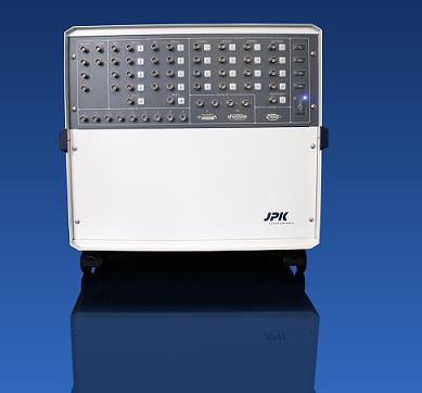 |
| JPK's new Vortis™ Advanced SPM Control System |
Abstract:
JPK Instruments, a world-leading manufacturer of nanoanalytic instrumentation in life sciences and soft matter announces the Vortis™ Advanced, the new standard in SPM Control systems with the lowest noise and highest signal speeds seen to date.
JPK Instruments announce the Vortis™ Advanced fully digital SPM Control Station
Berlin | Posted on September 8th, 2010Providing the highest performance of electronics controller for scanning probe microscopes, SPM, is one of the driving forces behind JPK's development programs. Recent engineering breakthroughs have enabled the elimination of DSP technology. JPK has utilized the new Power-PC hardware with the latest FPGA architecture to deliver the highest digital performance.
Vortis Advanced is now available with all of JPK's SPM systems: the NanoWizard® 3, the ForceRobot® 300 and the CellHesion® 200 now deliver even more superior results. With fast signal acquisition and control, advanced feedback and analysis are the keys for a modular and ultra flexible controller. The lowest noise levels are achieved using a new grounding concept, intelligent signal conditioning, temperature stabilized oscillators and passive cooling.
Vortis Advanced has been designed so the builder of their home-designed and built SPM heads may utilize these performance benefits. It comes with a large number of user accessible analog and digital signal channels, fast responding lock-in amplifiers and high end piezo drivers with closed loop control. Flexibility of design gives the user the ability to work with different probe configurations requiring different levels of control. For example, STM systems, systems using tuning forks and high frequency cantilevers all need very specific control, all of which are delivered by the Vortis Advanced. Synchronisation with external instruments including spectrometers, potentiostats and optical detection devices is provided too.
Control systems with the best hardware still require another vital element, powerful and modular software. JPK supplies the new package, SPMControl v4 to deliver ease of use plus the ability for user customized experiments through the implementation of many powerful data analysis and processing routines such as multi-channel oscilloscope functionality, advanced filtering, batch processing and channel overlay.
JPK develops, engineers and manufactures instrumentation in Germany to the world-recognised standards of German precision engineering, quality and functionality. For further details of the NanoWizard®3 and its many applications, please visit the JPK web site (www.jpk.com).
####
About JPK Instruments
JPK Instruments AG is a world-leading manufacturer of nanoanalytic instruments - particularly atomic force microscope (AFM) systems and optical tweezers - for a broad range of applications reaching from soft matter physics to nano-optics, from surface chemistry to cell and molecular biology. From its earliest days applying atomic force microscope (AFM) technology, JPK has recognized the opportunities provided by nanotechnology for transforming life sciences and soft matter research. This focus has driven JPK’s success in uniting the worlds of nanotechnology tools and life science applications by offering cutting-edge technology and unique applications expertise. Headquartered in Berlin and with direct operations in Dresden, Cambridge (UK), Singapore and Tokyo, JPK maintains a global network of distributors and support centers and provides on the spot applications and service support to an ever-growing community of researchers.
For more information, please click here
Contacts:
JPK Instruments AG
Bouchéstrasse 12
Haus 2, Aufgang C
Berlin 12435
Germany
T +49 30 5331 12070
F +49 30 5331 22555
NetDyaLog Limited
39 de Bohun Court
Saffron Walden
Essex CB10 2BA
T +44 (0) 1799 521881
M +44 (0) 7843 012997
Copyright © JPK Instruments
If you have a comment, please Contact us.Issuers of news releases, not 7th Wave, Inc. or Nanotechnology Now, are solely responsible for the accuracy of the content.
Bookmark:


| Related News Press |
News and information
![]() Simulating magnetization in a Heisenberg quantum spin chain April 5th, 2024
Simulating magnetization in a Heisenberg quantum spin chain April 5th, 2024
![]() NRL charters Navy’s quantum inertial navigation path to reduce drift April 5th, 2024
NRL charters Navy’s quantum inertial navigation path to reduce drift April 5th, 2024
![]() Discovery points path to flash-like memory for storing qubits: Rice find could hasten development of nonvolatile quantum memory April 5th, 2024
Discovery points path to flash-like memory for storing qubits: Rice find could hasten development of nonvolatile quantum memory April 5th, 2024
Announcements
![]() NRL charters Navy’s quantum inertial navigation path to reduce drift April 5th, 2024
NRL charters Navy’s quantum inertial navigation path to reduce drift April 5th, 2024
![]() Discovery points path to flash-like memory for storing qubits: Rice find could hasten development of nonvolatile quantum memory April 5th, 2024
Discovery points path to flash-like memory for storing qubits: Rice find could hasten development of nonvolatile quantum memory April 5th, 2024
Tools
![]() Ferroelectrically modulate the Fermi level of graphene oxide to enhance SERS response November 3rd, 2023
Ferroelectrically modulate the Fermi level of graphene oxide to enhance SERS response November 3rd, 2023
![]() The USTC realizes In situ electron paramagnetic resonance spectroscopy using single nanodiamond sensors November 3rd, 2023
The USTC realizes In situ electron paramagnetic resonance spectroscopy using single nanodiamond sensors November 3rd, 2023
|
|
||
|
|
||
| The latest news from around the world, FREE | ||
|
|
||
|
|
||
| Premium Products | ||
|
|
||
|
Only the news you want to read!
Learn More |
||
|
|
||
|
Full-service, expert consulting
Learn More |
||
|
|
||