Home > Press > Sarfus 3D-IMM: New equipement for nanometric sample charaterization in water
 |
Abstract:
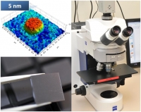
Nanolane is proud to announce the launch of its new equipment SARFUS 3D-IMM dedicated to the topographic characterization of nanometric samples in water.
Sarfus 3D-IMM: New equipement for nanometric sample charaterization in water
France | Posted on September 6th, 2010Equipments for characterization in water are still rare, relatively complex to operate and do not offer real-time images of samples. SARFUS 3D-IMM is designed to match the needs of the engineering and research community, especially in the Life Science but also in Thin Film and Surface Treatment areas. Indeed, SARFUS 3D-IMM is dedicated to the observation of nano-objects in real-time and to the thickness measurements of ultra-thin films in water.
Like the other SARFUS products, SARFUS 3D-IMM is based on SEEC optical technique that uses specific nonreflecting surfaces for cross-polarized reflected light microscopy. These surfaces -the Surfs- are used instead of standard microscope slides and generate a contrast enhancement of about 2 orders of magnitude, extending the application fields of optical microscopy toward the nanoworld.
Thanks to the absence of scanning and its easiness of use, SARFUS 3D-IMM equipment opens new perspectives for the nano-characterization in aqueous media by allowing dynamic studies of nanometric structures and rapid quality control of samples. In addition, the equipment is proposed with a powerful 3D topographic software for complete characterization (layer thicknesses, section profiles, roughnesses...) of nanometric samples.
The main applications concerned by this innovation are:
Biological objets
- Vesicles
- Lipid bilayers
- Biochips
- Cell adhesion
- ...
Thin films & Surface Treatment
- Polyelectrolytes
- Sensitive films (LCST)
- Nano-films
- Polymer patterns
- ...
The main features of SARFUS 3D-IMM equipment are:
- User friendly & Fast processing
- Repeatability : 0.1nm (according to ISO standard 17025)
- Z-sensibility limit: 0.2nm
- Range of measurement: 1 to 60nm
- Lateral resolution : 330nm
- Live video acquisition
- Time lapse (up to 15 image per second)
- Non destructive, no labelling
- Compatibility with fluorescence
####
About �olane
�olane is the signature, of seven companies, all gathered under 100% control of a holding, the �Financi�re de l�Ombr�e�, whose main activity is the conception, the study and the manufacture of professional electronic materials.
Each of them operates in complementary fields (technologies, industrial resource, economic sectors, and geographical areas). Strong synergies are present between them (conception, purchases, sales, industry, networks, and quality, to quote only the principal ones).
For more information, please click here
Contacts:
Nicolas Medard
Copyright © �olane
If you have a comment, please Contact us.Issuers of news releases, not 7th Wave, Inc. or Nanotechnology Now, are solely responsible for the accuracy of the content.
Bookmark:


| Related News Press |
News and information
![]() Simulating magnetization in a Heisenberg quantum spin chain April 5th, 2024
Simulating magnetization in a Heisenberg quantum spin chain April 5th, 2024
![]() NRL charters Navy�s quantum inertial navigation path to reduce drift April 5th, 2024
NRL charters Navy�s quantum inertial navigation path to reduce drift April 5th, 2024
![]() Discovery points path to flash-like memory for storing qubits: Rice find could hasten development of nonvolatile quantum memory April 5th, 2024
Discovery points path to flash-like memory for storing qubits: Rice find could hasten development of nonvolatile quantum memory April 5th, 2024
![]() Good as gold - improving infectious disease testing with gold nanoparticles April 5th, 2024
Good as gold - improving infectious disease testing with gold nanoparticles April 5th, 2024
Thin films
![]() Utilizing palladium for addressing contact issues of buried oxide thin film transistors April 5th, 2024
Utilizing palladium for addressing contact issues of buried oxide thin film transistors April 5th, 2024
![]() Understanding the mechanism of non-uniform formation of diamond film on tools: Paving the way to a dry process with less environmental impact March 24th, 2023
Understanding the mechanism of non-uniform formation of diamond film on tools: Paving the way to a dry process with less environmental impact March 24th, 2023
![]() New study introduces the best graphite films: The work by Distinguished Professor Feng Ding at UNIST has been published in the October 2022 issue of Nature Nanotechnology November 4th, 2022
New study introduces the best graphite films: The work by Distinguished Professor Feng Ding at UNIST has been published in the October 2022 issue of Nature Nanotechnology November 4th, 2022
Announcements
![]() NRL charters Navy�s quantum inertial navigation path to reduce drift April 5th, 2024
NRL charters Navy�s quantum inertial navigation path to reduce drift April 5th, 2024
![]() Discovery points path to flash-like memory for storing qubits: Rice find could hasten development of nonvolatile quantum memory April 5th, 2024
Discovery points path to flash-like memory for storing qubits: Rice find could hasten development of nonvolatile quantum memory April 5th, 2024
Tools
![]() Ferroelectrically modulate the Fermi level of graphene oxide to enhance SERS response November 3rd, 2023
Ferroelectrically modulate the Fermi level of graphene oxide to enhance SERS response November 3rd, 2023
![]() The USTC realizes In situ electron paramagnetic resonance spectroscopy using single nanodiamond sensors November 3rd, 2023
The USTC realizes In situ electron paramagnetic resonance spectroscopy using single nanodiamond sensors November 3rd, 2023
|
|
||
|
|
||
| The latest news from around the world, FREE | ||
|
|
||
|
|
||
| Premium Products | ||
|
|
||
|
Only the news you want to read!
Learn More |
||
|
|
||
|
Full-service, expert consulting
Learn More |
||
|
|
||