Home > Press > Notre Dame to Dedicate New Engineering Building
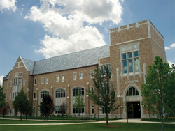 |
| Stinson-Remick Hall |
Abstract:
The University of Notre Dame will hold a ceremony Friday to dedicate a new engineering research facility. Stinson-Remick Hall will house a nanotechnology research center, the university's first semiconductor processing and device fabrication clean room and interdisciplinary learning center. The Midwest Institute for Nanoelectronics Discovery will also be located in the building.
Notre Dame to Dedicate New Engineering Building
South Bend, IN | Posted on September 2nd, 2010A new era in engineering research at the University of Notre Dame will be officially marked Friday (Sept. 4) with the dedication of Stinson-Remick Hall, a 142,000-square-foot facility that houses a nano technology research center, an 9,000-square-foot semiconductor processing and device fabrication clean room, and an undergraduate interdisciplinary learning center.
The building also houses Holy Cross Chapel, believed to be the only chapel inside a university engineering building in the country.
The dedication ceremonies will include a private Mass and a blessing of the building at 5 p.m.
The new building is called Stinson-Remick Hall in honor of principal benefactors Kenneth and Ann Stinson and Jack and Mary Ann Remick. Stinson is a 1964 Notre Dame graduate and a member of the Board of Trustees. Jack Remick, a 1959 graduate, is a member of the University's advisory council for the College of Engineering and a gift from Mary Ann Remick created an endowment for visiting fellows at Notre Dame's Center for Ethics and Culture.
The learning center is named in honor of major benefactors Ted and Tracy McCourtney. A 1960 Notre Dame graduate, Ted McCourtney is an emeritus member of the Board of Trustees.
Researchers in Notre Dame's Center for Nano Science and Technology explore new device concepts and associated architectures that are enabled by novel phenomena on the nanometer scale. Established in 1999, the center is under the direction of Wolfgang Porod, Frank. M Freimann Professor of Electrical Engineering.
The Notre Dame Energy Center was created in 2005 under the direction of Joan Brennecke, Keating-Crawford Professor of Chemical and Biomolecular Engineering. Faculty members associated with the center are seeking to develop new energy technologies, based on carbon dioxide sequestration in ionic liquids, new materials for nuclear energy utilization and related energy efficiency research to meet a compelling national and international challenge.
A major energy research program located in the building is a federal Energy Frontier Research Center led by Peter Burns and funded with an $18.5-million U.S. Department of Energy grant. Research at the center seeks to understand and control materials that contain actinides at the nanoscale. The research is intended to lay the scientific foundation for advanced nuclear energy systems that may provide much more energy while creating less nuclear waste.
Another initiative housed in Stinson-Remick is the Midwest Institute for Nanoelectronics Discovery (MIND), a consortium of academic, industry and government partners led by Notre Dame which explores and develops advanced devices, circuits and nanosystems with performance capabilities beyond conventional devices.
The interdisciplinary learning center is four times the size of its former location in Cushing Hall. The center provides undergraduate students with a blend of computer work stations, library resources and laboratory space.
The semiconductor processing and device fabrication clean room will be the first such facility at Notre Dame.
Stinson-Remick also is home to Notre Dame's Advanced Diagnostics and Therapeutics initiative (AD&T), an interdisciplinary research initiative focused on developing diagnostic and therapeutic technologies at the smallest molecular scales to address a diverse set of health and environmental challenges.
Also housed in Stinson-Remick is the Notre Dame Nanofabrication Facility (NDNF), which features comprehensive facilities for developing nano- and microelectronic materials and devices. NDNF serves approximately 150 researchers across the University each year as well as faculty from many others universities and research facilities across the country.
The new building also houses the Notre Dame Integrated Imaging Facility, which serves the science and engineering research communities by integrating three areas of the University's imaging expertise: electron microscopy, optical microscopy and in vivo imaging.
####
For more information, please click here
Copyright © University of Notre Dame
If you have a comment, please Contact us.Issuers of news releases, not 7th Wave, Inc. or Nanotechnology Now, are solely responsible for the accuracy of the content.
Bookmark:


| Related News Press |
News and information
![]() Simulating magnetization in a Heisenberg quantum spin chain April 5th, 2024
Simulating magnetization in a Heisenberg quantum spin chain April 5th, 2024
![]() NRL charters Navy�s quantum inertial navigation path to reduce drift April 5th, 2024
NRL charters Navy�s quantum inertial navigation path to reduce drift April 5th, 2024
![]() Discovery points path to flash-like memory for storing qubits: Rice find could hasten development of nonvolatile quantum memory April 5th, 2024
Discovery points path to flash-like memory for storing qubits: Rice find could hasten development of nonvolatile quantum memory April 5th, 2024
Videos/Movies
![]() New X-ray imaging technique to study the transient phases of quantum materials December 29th, 2022
New X-ray imaging technique to study the transient phases of quantum materials December 29th, 2022
![]() Solvent study solves solar cell durability puzzle: Rice-led project could make perovskite cells ready for prime time September 23rd, 2022
Solvent study solves solar cell durability puzzle: Rice-led project could make perovskite cells ready for prime time September 23rd, 2022
![]() Scientists prepare for the world�s smallest race: Nanocar Race II March 18th, 2022
Scientists prepare for the world�s smallest race: Nanocar Race II March 18th, 2022
![]() Visualizing the invisible: New fluorescent DNA label reveals nanoscopic cancer features March 4th, 2022
Visualizing the invisible: New fluorescent DNA label reveals nanoscopic cancer features March 4th, 2022
![]() OCSiAl receives the green light for Luxembourg graphene nanotube facility project to power the next generation of electric vehicles in Europe March 4th, 2022
OCSiAl receives the green light for Luxembourg graphene nanotube facility project to power the next generation of electric vehicles in Europe March 4th, 2022
Openings/New facilities/Groundbreaking/Expansion
![]() OCSiAl expands its graphene nanotube production capacities to Europe June 17th, 2022
OCSiAl expands its graphene nanotube production capacities to Europe June 17th, 2022
Govt.-Legislation/Regulation/Funding/Policy
![]() NRL charters Navy�s quantum inertial navigation path to reduce drift April 5th, 2024
NRL charters Navy�s quantum inertial navigation path to reduce drift April 5th, 2024
![]() Discovery points path to flash-like memory for storing qubits: Rice find could hasten development of nonvolatile quantum memory April 5th, 2024
Discovery points path to flash-like memory for storing qubits: Rice find could hasten development of nonvolatile quantum memory April 5th, 2024
![]() Chemical reactions can scramble quantum information as well as black holes April 5th, 2024
Chemical reactions can scramble quantum information as well as black holes April 5th, 2024
Academic/Education
![]() Rice University launches Rice Synthetic Biology Institute to improve lives January 12th, 2024
Rice University launches Rice Synthetic Biology Institute to improve lives January 12th, 2024
![]() Multi-institution, $4.6 million NSF grant to fund nanotechnology training September 9th, 2022
Multi-institution, $4.6 million NSF grant to fund nanotechnology training September 9th, 2022
Announcements
![]() NRL charters Navy�s quantum inertial navigation path to reduce drift April 5th, 2024
NRL charters Navy�s quantum inertial navigation path to reduce drift April 5th, 2024
![]() Discovery points path to flash-like memory for storing qubits: Rice find could hasten development of nonvolatile quantum memory April 5th, 2024
Discovery points path to flash-like memory for storing qubits: Rice find could hasten development of nonvolatile quantum memory April 5th, 2024
Energy
![]() Development of zinc oxide nanopagoda array photoelectrode: photoelectrochemical water-splitting hydrogen production January 12th, 2024
Development of zinc oxide nanopagoda array photoelectrode: photoelectrochemical water-splitting hydrogen production January 12th, 2024
![]() Shedding light on unique conduction mechanisms in a new type of perovskite oxide November 17th, 2023
Shedding light on unique conduction mechanisms in a new type of perovskite oxide November 17th, 2023
![]() Inverted perovskite solar cell breaks 25% efficiency record: Researchers improve cell efficiency using a combination of molecules to address different November 17th, 2023
Inverted perovskite solar cell breaks 25% efficiency record: Researchers improve cell efficiency using a combination of molecules to address different November 17th, 2023
![]() The efficient perovskite cells with a structured anti-reflective layer � another step towards commercialization on a wider scale October 6th, 2023
The efficient perovskite cells with a structured anti-reflective layer � another step towards commercialization on a wider scale October 6th, 2023
|
|
||
|
|
||
| The latest news from around the world, FREE | ||
|
|
||
|
|
||
| Premium Products | ||
|
|
||
|
Only the news you want to read!
Learn More |
||
|
|
||
|
Full-service, expert consulting
Learn More |
||
|
|
||