Home > Press > Raleigh/RTP to host the 43rd annual International Symposium on Microelectronics
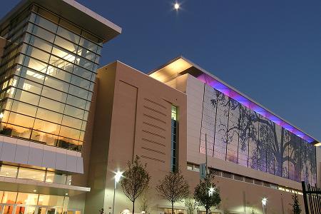 |
| Cree shimmer wall at the new Raleigh Convention Center where technical conference will be held |
Abstract:
IMAPS 2010 - International Conference and Exhibition on Microelectronics Showcases Advancements in Technologies Between the Chip and the System
Raleigh/RTP to host the 43rd annual International Symposium on Microelectronics
Raleigh, NC | Posted on July 31st, 2010The annual International Conference and Exhibition on Microelectronics returns to the U.S. East Coast this November, as leading scientists and engineers in the field of microelectronics gather in Raleigh/Research Triangle Park, NC on October 31 thru November 4, 2010 to showcase their work in a program of papers, panels, special sessions and an exhibition that will spotlight premier work in the fields of microelectronics, semiconductor packaging and circuit design. The 43rd International Symposium on Microelectronics will feature technical tracks on 3D Packaging/Interconnect, Design, Reliability, and Advanced Packaging & Materials.
This international technology forum for the presentation of applied research on microelectronics will be held at the new Raleigh Convention Center near Research Triangle Park, North Carolina, USA. More than 180 papers will be presented by researchers from corporations, universities and government labs worldwide.
Early registration ends on September 28, 2010, go to www.imaps.org for more information, or contact Michael O'Donoghue at
Sponsored by the International Microelectronics And Packaging Society (IMAPS), the International Symposium on Microelectronics is the largest society dedicated to the advancement and growth of microelectronics and electronics packaging technologies through professional education.
####
About IMAPS
Founded in 1967, IMAPS is the leading international microelectronics and electronic packaging society with professional members in 23 North American chapters and 21 international chapters. Members of the Society represent every discipline and specialty in the electronics industry and include both technical and marketing professionals. IMAPS leads the Microelectronics Packaging, Interconnect and Assembly Community, providing means of communicating, educating and interacting at all levels. The Society's portfolio of technologies is disseminated through symposia, conferences, workshops, professional development courses and other efforts. IMAPS currently has more than 4,000 members in the United States and more than 4,000 international members around the world.
For more information, please click here
Contacts:
Editor Contacts:
Chris Burke or Garth Miller
BtB Marketing Communications
(919) 872-8172
Copyright © IMAPS
If you have a comment, please Contact us.Issuers of news releases, not 7th Wave, Inc. or Nanotechnology Now, are solely responsible for the accuracy of the content.
Bookmark:


| Related News Press |
News and information
![]() Simulating magnetization in a Heisenberg quantum spin chain April 5th, 2024
Simulating magnetization in a Heisenberg quantum spin chain April 5th, 2024
![]() NRL charters Navy�s quantum inertial navigation path to reduce drift April 5th, 2024
NRL charters Navy�s quantum inertial navigation path to reduce drift April 5th, 2024
![]() Discovery points path to flash-like memory for storing qubits: Rice find could hasten development of nonvolatile quantum memory April 5th, 2024
Discovery points path to flash-like memory for storing qubits: Rice find could hasten development of nonvolatile quantum memory April 5th, 2024
Chip Technology
![]() Discovery points path to flash-like memory for storing qubits: Rice find could hasten development of nonvolatile quantum memory April 5th, 2024
Discovery points path to flash-like memory for storing qubits: Rice find could hasten development of nonvolatile quantum memory April 5th, 2024
![]() Utilizing palladium for addressing contact issues of buried oxide thin film transistors April 5th, 2024
Utilizing palladium for addressing contact issues of buried oxide thin film transistors April 5th, 2024
![]() HKUST researchers develop new integration technique for efficient coupling of III-V and silicon February 16th, 2024
HKUST researchers develop new integration technique for efficient coupling of III-V and silicon February 16th, 2024
Announcements
![]() NRL charters Navy�s quantum inertial navigation path to reduce drift April 5th, 2024
NRL charters Navy�s quantum inertial navigation path to reduce drift April 5th, 2024
![]() Discovery points path to flash-like memory for storing qubits: Rice find could hasten development of nonvolatile quantum memory April 5th, 2024
Discovery points path to flash-like memory for storing qubits: Rice find could hasten development of nonvolatile quantum memory April 5th, 2024
Events/Classes
![]() Researchers demonstrate co-propagation of quantum and classical signals: Study shows that quantum encryption can be implemented in existing fiber networks January 20th, 2023
Researchers demonstrate co-propagation of quantum and classical signals: Study shows that quantum encryption can be implemented in existing fiber networks January 20th, 2023
|
|
||
|
|
||
| The latest news from around the world, FREE | ||
|
|
||
|
|
||
| Premium Products | ||
|
|
||
|
Only the news you want to read!
Learn More |
||
|
|
||
|
Full-service, expert consulting
Learn More |
||
|
|
||