Home > Press > Phenom Pro Suite
 |
Abstract:
Phenom Pro Suite generates answers not just images
Phenom Pro Suite
Eindhoven, The Netherlands | Posted on July 21st, 2010Phenom-World BV, producer of the Phenom desktop scanning electron microscope, announces the launch of a new software product, the Phenom Pro Suite.
The Phenom Pro Suite applications expand the functionality of the Phenom by automated collection of images, visualize samples in 3D, measure surface roughness and automated fiber analysis.
With the introduction of the Phenom Pro Suite the following four applications will be available:
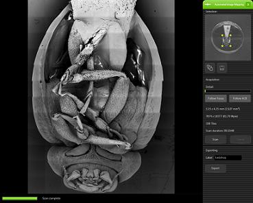
Automated Image Mapping
The Automated Image Mapping application enables users to automatically collect multiple images in a regular grid from the Phenom desktop scanning electron microscope. The Automated Image Mapping application software will create a larger field of view or a high-resolution image map.
Remote User Interface
Phenom Pro Suite's Remote User Interface makes it possible to access the Phenom from a different location. You can control the Phenom and all its common features, image your sample, take images and store them on a USB, network location or your local hard drive.
3D Roughness Reconstruction
With the 3D Roughness Reconstruction application, it is possible to generate three-dimensional images and sub micrometer roughness measurements. This fully automated application will help to communicate imaging results and will extract and visualize data normally hidden within a sample.
Fibermetric
Direct observation and measurement of micro and nano fibers is faster, better and easier than ever before. Fibermetric automatically collects hundreds of data points to provide a solid statistical analysis and size distribution of fiber and filter samples.
Phenom-World focuses on supporting their customers with answers and will create more applications for the Phenom Pro Suite in the near future.
####
About Phenom-World
Phenom-World produces, services and develops electron beam-based analytical products.
Located in the high-tech region of Eindhoven in the Netherlands, Phenom-World is well positioned to press ahead with product innovations.
With sales representatives in more than 30 countries around the world, Phenom-World has a strong global presence to address the desktop scanning electron microscopy market. Phenom-World BV is a joint venture of the NTS Group (system supplier to high-tech industries), Sioux (a supplier of trend-setting services and products for embedded systems, medical systems and remote solutions), and FEI (the premier provider of high end electron and ion-beam microscopes).
For more information, please click here
Contacts:
Dillenburgstraat 9E 5652AM, Eindhoven The Netherlands
Phone: +31 (0)40 259 7360
Copyright © Phenom-World
If you have a comment, please Contact us.Issuers of news releases, not 7th Wave, Inc. or Nanotechnology Now, are solely responsible for the accuracy of the content.
Bookmark:


| Related News Press |
News and information
![]() Simulating magnetization in a Heisenberg quantum spin chain April 5th, 2024
Simulating magnetization in a Heisenberg quantum spin chain April 5th, 2024
![]() NRL charters Navy�s quantum inertial navigation path to reduce drift April 5th, 2024
NRL charters Navy�s quantum inertial navigation path to reduce drift April 5th, 2024
![]() Discovery points path to flash-like memory for storing qubits: Rice find could hasten development of nonvolatile quantum memory April 5th, 2024
Discovery points path to flash-like memory for storing qubits: Rice find could hasten development of nonvolatile quantum memory April 5th, 2024
Announcements
![]() NRL charters Navy�s quantum inertial navigation path to reduce drift April 5th, 2024
NRL charters Navy�s quantum inertial navigation path to reduce drift April 5th, 2024
![]() Discovery points path to flash-like memory for storing qubits: Rice find could hasten development of nonvolatile quantum memory April 5th, 2024
Discovery points path to flash-like memory for storing qubits: Rice find could hasten development of nonvolatile quantum memory April 5th, 2024
Tools
![]() Ferroelectrically modulate the Fermi level of graphene oxide to enhance SERS response November 3rd, 2023
Ferroelectrically modulate the Fermi level of graphene oxide to enhance SERS response November 3rd, 2023
![]() The USTC realizes In situ electron paramagnetic resonance spectroscopy using single nanodiamond sensors November 3rd, 2023
The USTC realizes In situ electron paramagnetic resonance spectroscopy using single nanodiamond sensors November 3rd, 2023
|
|
||
|
|
||
| The latest news from around the world, FREE | ||
|
|
||
|
|
||
| Premium Products | ||
|
|
||
|
Only the news you want to read!
Learn More |
||
|
|
||
|
Full-service, expert consulting
Learn More |
||
|
|
||