Home > Press > New Cold Field Emission Gun Enhances Ultrahigh Atomic Level Resolution of JEOL ARM200F Aberration-Corrected S/TEM
 |
Abstract:
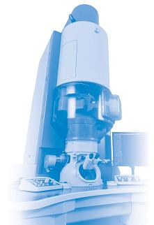
JEOL USA is pleased to announce that a new Cold Field Emission Gun is now available for the atomic resolution analytical JEM-ARM200F Transmission Electron Microscope (TEM). The ARM200F, introduced in 2009, has set a new benchmark for advanced aberration-corrected S/TEM technology with the highest resolution commercially available in its class.
New Cold Field Emission Gun Enhances Ultrahigh Atomic Level Resolution of JEOL ARM200F Aberration-Corrected S/TEM
Peabody, MA | Posted on July 21st, 2010Now outfitted with the optional and field-retrofittable Cold FEG, the ARM200F's ultrahigh imaging resolution is guaranteed at 78 picometers with an energy resolution of 0.3 eV. The higher brightness and smaller source size of the Cold FEG produce a smaller, sharper electron probe with a dramatically larger probe current, resulting in enhanced atom-by-atom imaging and chemical analysis. Additionally, the narrow energy spread of the electrons emitted from the Cold FEG enables atomic resolution analysis of EELS fine structures, which can be used to determine such things as electronic properties. Ultra-high vacuum near the electron source assures high stability of the electron probe current while high electrical system stability of 10-7 maintains the very narrow energy spread of the electron probe.
"The addition of a cold FEG to the ARM family adds another arrow to the JEOL quiver for atomic scale imaging and characterization. This enhancement makes it possible to perform sub-Angstrom imaging and atomic column chemistry with accuracy, speed and ease never seen before," said Dr. Thomas Isabell, Director of the TEM Product Division at JEOL USA.
The JEOL ARM200F electron column integrates the Cold FEG, S/TEM and Cs correction in an unparalleled, ultra-stable design. Superior shielding safeguards the ultrahigh-powered optics from airflow, vibration, acoustical, magnetic, electronic, and thermal interferences.
The first ARM200F with Cold FEG in the USA will be installed at Florida State University's Applied Superconductivity Center, housed in the National High Magnetic Field Laboratory.
####
About JEOL
JEOL is a world leader in electron optical equipment and instrumentation for high-end scientific and industrial research and development. Core product groups include electron microscopes (SEMs and TEMs), instruments for the semiconductor industry (electron beam lithography and a series of defect review and inspection tools), and analytical instruments including mass spectrometers, NMRs and ESRs.
JEOL USA, Inc., a wholly owned subsidiary of JEOL, Ltd., Japan, was incorporated in the United States in 1962. The company has 13 regional service centers that offer unlimited emergency service and support in the U.S.
For more information, please click here
Contacts:
Editorial Contact:
Patricia Corkum
Marketing Manager
978-536-2273
Pamela Mansfield
JEOL USA
11 Dearborn Road
Peabody, MA 01960
978-536-2309
Copyright © JEOL
If you have a comment, please Contact us.Issuers of news releases, not 7th Wave, Inc. or Nanotechnology Now, are solely responsible for the accuracy of the content.
Bookmark:


| Related News Press |
News and information
![]() Simulating magnetization in a Heisenberg quantum spin chain April 5th, 2024
Simulating magnetization in a Heisenberg quantum spin chain April 5th, 2024
![]() NRL charters Navy�s quantum inertial navigation path to reduce drift April 5th, 2024
NRL charters Navy�s quantum inertial navigation path to reduce drift April 5th, 2024
![]() Discovery points path to flash-like memory for storing qubits: Rice find could hasten development of nonvolatile quantum memory April 5th, 2024
Discovery points path to flash-like memory for storing qubits: Rice find could hasten development of nonvolatile quantum memory April 5th, 2024
Announcements
![]() NRL charters Navy�s quantum inertial navigation path to reduce drift April 5th, 2024
NRL charters Navy�s quantum inertial navigation path to reduce drift April 5th, 2024
![]() Discovery points path to flash-like memory for storing qubits: Rice find could hasten development of nonvolatile quantum memory April 5th, 2024
Discovery points path to flash-like memory for storing qubits: Rice find could hasten development of nonvolatile quantum memory April 5th, 2024
Tools
![]() Ferroelectrically modulate the Fermi level of graphene oxide to enhance SERS response November 3rd, 2023
Ferroelectrically modulate the Fermi level of graphene oxide to enhance SERS response November 3rd, 2023
![]() The USTC realizes In situ electron paramagnetic resonance spectroscopy using single nanodiamond sensors November 3rd, 2023
The USTC realizes In situ electron paramagnetic resonance spectroscopy using single nanodiamond sensors November 3rd, 2023
|
|
||
|
|
||
| The latest news from around the world, FREE | ||
|
|
||
|
|
||
| Premium Products | ||
|
|
||
|
Only the news you want to read!
Learn More |
||
|
|
||
|
Full-service, expert consulting
Learn More |
||
|
|
||