Home > Press > Chemists Grow Crystals with a Twist—and Untwist
 |
| NYU and St. Petersburg State University chemists have discovered a wholly new phenomenon for crystal growth—a crystal that continually changes its shape as it grows. |
Abstract:
Chemists from New York University and Russia's St. Petersburg State University have created crystals that can twist and untwist, pointing to a much more varied process of crystal growth than previously thought.
Chemists Grow Crystals with a Twist—and Untwist
Manhattan, NY | Posted on July 20th, 2010Their work, which appears in the latest issue of the Journal of the American Chemical Society, may explain some of the properties of high-polymers, which are used in clothing and liquid crystal displays, among other consumer products.
Crystal growth has traditionally been viewed as a collection of individual atoms, molecules, or small clusters adding to a larger block that remains in a fixed translational relationship to the rest.
But the NYU and St. Petersburg State University chemists discovered a wholly new phenomenon for growth—a crystal that continually changes its shape as it grows.
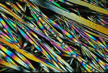
To do this, the researchers focused on crystals from hippuric acid—a derivative of the amino acid glycine. As molecules were added to the end of fine crystalline needles, stresses built up at the tips of the crystals and resulted in a helical twist—much like DNA's double helix. The process was reversed when crystals thickened from the opposite end of the growing tip—that is, the crystals stiffened, thereby undoing the twisted formations. This is because the elasticity of the crystals decreases as they become thicker, thus "squeezing out" the deformations that were induced at the growing tip.
"This competition between twisting and untwisting creates needles with a rainbow of colors, which is a characteristic of tightly wound helices, as well as ribbons that have become completely untwisted," said Bart Kahr, one of the study's co-authors and a professor in NYU's Department of Chemistry, explaining the crystals' appearance. "This is a very strange and new perspective on crystal growth."
"This dynamic has not been observed before and points to a much more active process of crystal growth than we had anticipated," added Kahr, also part of NYU's Molecular Design Institute.
The work's other co-authors were Alexander Shtukenberg, a senior researcher from Russia's St. Petersburg State University and a visiting scholar at NYU, and John Freudenthal, an NYU doctoral student.
####
For more information, please click here
Contacts:
James Devitt
(212) 998-6808
Copyright © New York University
If you have a comment, please Contact us.Issuers of news releases, not 7th Wave, Inc. or Nanotechnology Now, are solely responsible for the accuracy of the content.
Bookmark:


| Related News Press |
News and information
![]() Simulating magnetization in a Heisenberg quantum spin chain April 5th, 2024
Simulating magnetization in a Heisenberg quantum spin chain April 5th, 2024
![]() NRL charters Navy’s quantum inertial navigation path to reduce drift April 5th, 2024
NRL charters Navy’s quantum inertial navigation path to reduce drift April 5th, 2024
![]() Discovery points path to flash-like memory for storing qubits: Rice find could hasten development of nonvolatile quantum memory April 5th, 2024
Discovery points path to flash-like memory for storing qubits: Rice find could hasten development of nonvolatile quantum memory April 5th, 2024
![]() Good as gold - improving infectious disease testing with gold nanoparticles April 5th, 2024
Good as gold - improving infectious disease testing with gold nanoparticles April 5th, 2024
Display technology/LEDs/SS Lighting/OLEDs
![]() Utilizing palladium for addressing contact issues of buried oxide thin film transistors April 5th, 2024
Utilizing palladium for addressing contact issues of buried oxide thin film transistors April 5th, 2024
Chemistry
![]() What heat can tell us about battery chemistry: using the Peltier effect to study lithium-ion cells March 8th, 2024
What heat can tell us about battery chemistry: using the Peltier effect to study lithium-ion cells March 8th, 2024
![]() Nanoscale CL thermometry with lanthanide-doped heavy-metal oxide in TEM March 8th, 2024
Nanoscale CL thermometry with lanthanide-doped heavy-metal oxide in TEM March 8th, 2024
Academic/Education
![]() Rice University launches Rice Synthetic Biology Institute to improve lives January 12th, 2024
Rice University launches Rice Synthetic Biology Institute to improve lives January 12th, 2024
![]() Multi-institution, $4.6 million NSF grant to fund nanotechnology training September 9th, 2022
Multi-institution, $4.6 million NSF grant to fund nanotechnology training September 9th, 2022
Discoveries
![]() Chemical reactions can scramble quantum information as well as black holes April 5th, 2024
Chemical reactions can scramble quantum information as well as black holes April 5th, 2024
![]() New micromaterial releases nanoparticles that selectively destroy cancer cells April 5th, 2024
New micromaterial releases nanoparticles that selectively destroy cancer cells April 5th, 2024
![]() Utilizing palladium for addressing contact issues of buried oxide thin film transistors April 5th, 2024
Utilizing palladium for addressing contact issues of buried oxide thin film transistors April 5th, 2024
Announcements
![]() NRL charters Navy’s quantum inertial navigation path to reduce drift April 5th, 2024
NRL charters Navy’s quantum inertial navigation path to reduce drift April 5th, 2024
![]() Discovery points path to flash-like memory for storing qubits: Rice find could hasten development of nonvolatile quantum memory April 5th, 2024
Discovery points path to flash-like memory for storing qubits: Rice find could hasten development of nonvolatile quantum memory April 5th, 2024
Textiles/Clothing
![]() Protective equipment with graphene nanotubes meets the strictest ESD safety standards March 25th, 2022
Protective equipment with graphene nanotubes meets the strictest ESD safety standards March 25th, 2022
![]() Polymer fibers with graphene nanotubes make it possible to heat hard-to-reach, complex-shaped items February 11th, 2022
Polymer fibers with graphene nanotubes make it possible to heat hard-to-reach, complex-shaped items February 11th, 2022
![]() Flexible material shows potential for use in fabrics to heat, cool July 3rd, 2020
Flexible material shows potential for use in fabrics to heat, cool July 3rd, 2020
Research partnerships
![]() Discovery points path to flash-like memory for storing qubits: Rice find could hasten development of nonvolatile quantum memory April 5th, 2024
Discovery points path to flash-like memory for storing qubits: Rice find could hasten development of nonvolatile quantum memory April 5th, 2024
![]() Researchers’ approach may protect quantum computers from attacks March 8th, 2024
Researchers’ approach may protect quantum computers from attacks March 8th, 2024
![]() 'Sudden death' of quantum fluctuations defies current theories of superconductivity: Study challenges the conventional wisdom of superconducting quantum transitions January 12th, 2024
'Sudden death' of quantum fluctuations defies current theories of superconductivity: Study challenges the conventional wisdom of superconducting quantum transitions January 12th, 2024
|
|
||
|
|
||
| The latest news from around the world, FREE | ||
|
|
||
|
|
||
| Premium Products | ||
|
|
||
|
Only the news you want to read!
Learn More |
||
|
|
||
|
Full-service, expert consulting
Learn More |
||
|
|
||