Home > Press > Small wires make big connections for microelectronics
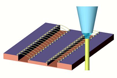 |
| Illinois researchers can make tiny wire bonds to connect integrated chips using a direct-write technique. A micropipette nozzle is like a tiny fountain pen writes the wire bonds in 3-D space with metal instead of ink. Image courtesy Min-Feng Yu |
Abstract:
University of Illinois engineers have developed a novel direct-writing method for manufacturing metal interconnects that could shrink integrated circuits and expand microelectronics.
Small wires make big connections for microelectronics
Champaign, IL | Posted on July 16th, 2010Integrated chips are made by wiring multiple transistors and electronic components together to perform complex functions. The connections between chips and circuit boards traditionally are made from pre-fabricated metal wires that connect to a designated bonding pad on a chip.
"Integrated functions require many wire connections. It's tedious and time-consuming to make and increases cost," said Min-Feng Yu, a professor of mechanical science and engineering at Illinois.
In addition, the bonding pad for traditional wire bonds takes up a substantial area of space. As technology has moved toward smaller electronics, shrinking wiring has been a substantial obstacle. Many microelectronic devices are much smaller than the required 50-by-50 micron square bonding site, prohibiting integrated functions on the very small scale.
"There's no existing cost-effective technology that would allow you to wire-bond microstructures," said Yu, "so let's get rid of those wires, and instead, why not directly produce them on-site between the connection points?"
Yu and graduate student Jie Hu developed a direct-write technique that produces tiny pure metal wires much smaller in diameter than traditional wires and requiring two orders of magnitude less bonding area. In a paper appearing in the July 16 edition of Science, they demonstrate as many as 20 of their new wires bonded to a single standard bonding site.
"This technique means the pads can be much smaller than what's needed for traditional wire-bonding technology," Yu said. This reduction in area could allow manufacturers to produce more chips per wafer of semiconductor material. It could also enable more complex integrated functions in microelectronics.
The pair have demonstrated their technique with both copper and platinum wires, and plan to explore the technique with other metals.
Yu likens their technique to writing with a fountain pen. "People's mindset is that you draw a line on a surface, but what we're doing is writing to 3-D space," he said.
The duo loaded a micropipette - a device that dispenses tiny amounts of liquid - with a copper electrolyte solution. When the pipette comes into close contact with the surface, a liquid bridge forms between the pipette tip and the bonding pad. The researchers then apply an electric current, which causes the copper in the solution to deposit as solid metal. As the tip moves through space, copper continues to deposit from the solution in the pipette, like ink from a pen, creating a wire. The challenge for Yu and Hu was calculating the correct speed to move the pipette tip to maintain the liquid bridge between the nozzle and the growing wire.
"It's liquid, so it can easily be shaped," Yu said. "As long as you maintain your speed within a certain range, you will always be able to produce uniform, high-quality wires."
They also had to figure out how to "write" the wires laterally for chip-to-chip bonding. Typical micropipette nozzles are flat at the end, but too much tilting breaks the liquid contact. The Illinois duo found that a notched nozzle, with a 90-degree cut in the side, allowed lateral movement, meaning that the wires can arc from one bonding site to another, even if the chips are stacked or tiered.
The process is automated, so Yu hopes to develop arrays of micropipettes to produce wire bonds in bulk for more efficient manufacturing.
"An advantage is that you can do this in parallel," he said. "Instead of one nozzle, suppose you have 10, 20 or 100 working simultaneously. In one step, you can make tens or hundreds of bonds, and that is cost-saving."
In addition to wire bonds, the technique could produce a myriad of metal microstructures for various applications.
"The ability to fabricate metallic structures in 3-D can open up many other opportunities," Yu said. "It has lots of desirable properties aside from the electrical ones. You can imagine the structures that take advantage of the different properties of metal."
####
For more information, please click here
Contacts:
Min-Feng Yu
217-333-9246
Liz Ahlberg
Physical Sciences Editor
217-244-1073
Copyright © University of Illinois at Urbana-Champaign
If you have a comment, please Contact us.Issuers of news releases, not 7th Wave, Inc. or Nanotechnology Now, are solely responsible for the accuracy of the content.
Bookmark:


| Related News Press |
News and information
![]() Simulating magnetization in a Heisenberg quantum spin chain April 5th, 2024
Simulating magnetization in a Heisenberg quantum spin chain April 5th, 2024
![]() NRL charters Navy�s quantum inertial navigation path to reduce drift April 5th, 2024
NRL charters Navy�s quantum inertial navigation path to reduce drift April 5th, 2024
![]() Discovery points path to flash-like memory for storing qubits: Rice find could hasten development of nonvolatile quantum memory April 5th, 2024
Discovery points path to flash-like memory for storing qubits: Rice find could hasten development of nonvolatile quantum memory April 5th, 2024
Possible Futures
![]() Discovery points path to flash-like memory for storing qubits: Rice find could hasten development of nonvolatile quantum memory April 5th, 2024
Discovery points path to flash-like memory for storing qubits: Rice find could hasten development of nonvolatile quantum memory April 5th, 2024
![]() With VECSELs towards the quantum internet Fraunhofer: IAF achieves record output power with VECSEL for quantum frequency converters April 5th, 2024
With VECSELs towards the quantum internet Fraunhofer: IAF achieves record output power with VECSEL for quantum frequency converters April 5th, 2024
Chip Technology
![]() Discovery points path to flash-like memory for storing qubits: Rice find could hasten development of nonvolatile quantum memory April 5th, 2024
Discovery points path to flash-like memory for storing qubits: Rice find could hasten development of nonvolatile quantum memory April 5th, 2024
![]() Utilizing palladium for addressing contact issues of buried oxide thin film transistors April 5th, 2024
Utilizing palladium for addressing contact issues of buried oxide thin film transistors April 5th, 2024
![]() HKUST researchers develop new integration technique for efficient coupling of III-V and silicon February 16th, 2024
HKUST researchers develop new integration technique for efficient coupling of III-V and silicon February 16th, 2024
Nanoelectronics
![]() Interdisciplinary: Rice team tackles the future of semiconductors Multiferroics could be the key to ultralow-energy computing October 6th, 2023
Interdisciplinary: Rice team tackles the future of semiconductors Multiferroics could be the key to ultralow-energy computing October 6th, 2023
![]() Key element for a scalable quantum computer: Physicists from Forschungszentrum J�lich and RWTH Aachen University demonstrate electron transport on a quantum chip September 23rd, 2022
Key element for a scalable quantum computer: Physicists from Forschungszentrum J�lich and RWTH Aachen University demonstrate electron transport on a quantum chip September 23rd, 2022
![]() Reduced power consumption in semiconductor devices September 23rd, 2022
Reduced power consumption in semiconductor devices September 23rd, 2022
![]() Atomic level deposition to extend Moore�s law and beyond July 15th, 2022
Atomic level deposition to extend Moore�s law and beyond July 15th, 2022
Announcements
![]() NRL charters Navy�s quantum inertial navigation path to reduce drift April 5th, 2024
NRL charters Navy�s quantum inertial navigation path to reduce drift April 5th, 2024
![]() Discovery points path to flash-like memory for storing qubits: Rice find could hasten development of nonvolatile quantum memory April 5th, 2024
Discovery points path to flash-like memory for storing qubits: Rice find could hasten development of nonvolatile quantum memory April 5th, 2024
|
|
||
|
|
||
| The latest news from around the world, FREE | ||
|
|
||
|
|
||
| Premium Products | ||
|
|
||
|
Only the news you want to read!
Learn More |
||
|
|
||
|
Full-service, expert consulting
Learn More |
||
|
|
||