Home > Press > How soccer ball molecules push their way under surfaces
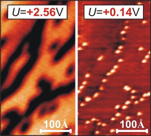 |
| Microscopical image of a graphene layer on a nickel substrate. The image to the left, which was measured at an arbitrary bias voltage of the microscope tip, shows just dark stripes. Only after the bias voltage has spectroscopically been tuned to the very C60 molecules (right), they become visible beneath the graphene layer as the cause of the stripe pattern. |
Abstract:
HZB researchers observe atomic processes while doping semiconductor materials
How soccer ball molecules push their way under surfaces
Berlin | Posted on July 13th, 2010Fullerene and graphene, two forms of carbon only recently discovered, have been stimulating the imaginations of researchers ever since their discovery (fullerene in 1970, graphene in 2004). With graphene especially, researchers see a chance for a new chapter in electronics, since this semiconductor material could one day replace the long-standing key element silicon. For this to happen, it would have to be possible to dope graphene - which is a single-atom layer of graphite - with foreign atoms. And in such a way that the important structural properties of graphene remain intact. In the online preprint of August issue of the journal Advanced Materials (DOI: 10.1002/adma. 201000695) researchers from Helmholtz-Zentrum Berlin f�r Materialien und Energie (HZB) report on a new technique of microscopy. With it, they can show how individual fullerene molecules used for doping push their way under a graphene layer that has been previously deposited onto a nickel substrate.
Graphene is the first crystal known to be stable in two dimensions, because its carbon atoms arrange themselves into a honeycomb structure of hexagons. Fullerene has the addition of pentagons, allowing a spherical structure for which the 60-carbon-atom molecule has made its name as the soccer ball molecule.
Andrei Varykhalov and colleagues deposited a thin layer of graphene onto a nickel substrate using chemical vapour deposition starting with propylene. Next, they inserted individual fullerene molecules between the nickel surface and the graphene layer. They achieved this by rapidly heating the sample to 400 degrees Celsius, followed by brief annealing. The crucial technique that allowed them to observe the fullerene molecules as they squeezed their way in - a process called intercalation - was scanning tunnelling microscopy.
An electrically conductive stylus tip is systematically scanned over the sample surface, which is also conductive. Yet, the tip and object surface never come into contact, so no current flows at first. When the microscope tip comes to within a few tenths of a nanometre of the sample surface, however, the tunnel-ling effect kicks in. That means an exchange of electrons from the sample sur-face and tip starts to take place. If a voltage is then applied, a tunnel current flows, which responds with utmost sensitivity to the tiniest changes in distance.
The HZB researchers set up their scanning tunnelling microscopy experiment such that a clear contrast shows up as soon as the tip of the microscope per-ceives the fullerene molecules beneath the graphene surface. To obtain crucial parameters for this, they first studied the sample using synchrotron radiation at the storage ring BESSY II.
"Using our imaging technique, we can visualize intercalation compounds quite universally," Andrei Varykhalov emphasizes the importance of the experiments. In the development of new semiconductor technology, such an imaging tech-nique is indispensable for developing new components.
####
About Helmholtz-Zentrum Berlin
The Helmholtz-Zentrum Berlin f�r Materialien und Energie (HZB) operates and develops large scale facilities for research with photons (synchrotron beams) and neutrons. The experimental facilities, some of which are unique, are used annually by more than 2,500 guest researchers from universities and other research organisations worldwide. Above all, HZB is known for the unique sam-ple environments that can be created (high magnetic fields, low temperatures). HZB conducts materials research on themes that espe-cially benefit from and are suited to large scale facilities. Research topics include magnetic materials and functional materials.
In the research focus area of solar energy, the development of thin film solar cells is a priority, whilst chemical fuels from sunlight are also a vital research theme. HZB has approx.1,100 employees of whom some 800 work on the Lise-Meitner Campus in Wannsee and 300 on the Wilhelm-Conrad-R�ntgen Campus in Adlershof.
HZB is a member of the Helmholtz Association of German Research Centres, the largest scientific organisation in Germany.
For more information, please click here
Contacts:
Dr. Andrei Varykhalov
(030) 8062-14888
Priv.-Doz. Dr. Oliver Rader
(030) 8062-12950
Press Office
Dr. Ina Helms
(030) 8062-42034
Copyright © Helmholtz-Zentrum Berlin
If you have a comment, please Contact us.Issuers of news releases, not 7th Wave, Inc. or Nanotechnology Now, are solely responsible for the accuracy of the content.
Bookmark:


| Related News Press |
News and information
![]() Simulating magnetization in a Heisenberg quantum spin chain April 5th, 2024
Simulating magnetization in a Heisenberg quantum spin chain April 5th, 2024
![]() NRL charters Navy�s quantum inertial navigation path to reduce drift April 5th, 2024
NRL charters Navy�s quantum inertial navigation path to reduce drift April 5th, 2024
![]() Discovery points path to flash-like memory for storing qubits: Rice find could hasten development of nonvolatile quantum memory April 5th, 2024
Discovery points path to flash-like memory for storing qubits: Rice find could hasten development of nonvolatile quantum memory April 5th, 2024
![]() Good as gold - improving infectious disease testing with gold nanoparticles April 5th, 2024
Good as gold - improving infectious disease testing with gold nanoparticles April 5th, 2024
Thin films
![]() Utilizing palladium for addressing contact issues of buried oxide thin film transistors April 5th, 2024
Utilizing palladium for addressing contact issues of buried oxide thin film transistors April 5th, 2024
Chemistry
![]() What heat can tell us about battery chemistry: using the Peltier effect to study lithium-ion cells March 8th, 2024
What heat can tell us about battery chemistry: using the Peltier effect to study lithium-ion cells March 8th, 2024
![]() Nanoscale CL thermometry with lanthanide-doped heavy-metal oxide in TEM March 8th, 2024
Nanoscale CL thermometry with lanthanide-doped heavy-metal oxide in TEM March 8th, 2024
Possible Futures
![]() Discovery points path to flash-like memory for storing qubits: Rice find could hasten development of nonvolatile quantum memory April 5th, 2024
Discovery points path to flash-like memory for storing qubits: Rice find could hasten development of nonvolatile quantum memory April 5th, 2024
![]() With VECSELs towards the quantum internet Fraunhofer: IAF achieves record output power with VECSEL for quantum frequency converters April 5th, 2024
With VECSELs towards the quantum internet Fraunhofer: IAF achieves record output power with VECSEL for quantum frequency converters April 5th, 2024
Academic/Education
![]() Rice University launches Rice Synthetic Biology Institute to improve lives January 12th, 2024
Rice University launches Rice Synthetic Biology Institute to improve lives January 12th, 2024
![]() Multi-institution, $4.6 million NSF grant to fund nanotechnology training September 9th, 2022
Multi-institution, $4.6 million NSF grant to fund nanotechnology training September 9th, 2022
Chip Technology
![]() Discovery points path to flash-like memory for storing qubits: Rice find could hasten development of nonvolatile quantum memory April 5th, 2024
Discovery points path to flash-like memory for storing qubits: Rice find could hasten development of nonvolatile quantum memory April 5th, 2024
![]() Utilizing palladium for addressing contact issues of buried oxide thin film transistors April 5th, 2024
Utilizing palladium for addressing contact issues of buried oxide thin film transistors April 5th, 2024
![]() HKUST researchers develop new integration technique for efficient coupling of III-V and silicon February 16th, 2024
HKUST researchers develop new integration technique for efficient coupling of III-V and silicon February 16th, 2024
Nanotubes/Buckyballs/Fullerenes/Nanorods/Nanostrings
![]() Tests find no free-standing nanotubes released from tire tread wear September 8th, 2023
Tests find no free-standing nanotubes released from tire tread wear September 8th, 2023
![]() Detection of bacteria and viruses with fluorescent nanotubes July 21st, 2023
Detection of bacteria and viruses with fluorescent nanotubes July 21st, 2023
Nanoelectronics
![]() Interdisciplinary: Rice team tackles the future of semiconductors Multiferroics could be the key to ultralow-energy computing October 6th, 2023
Interdisciplinary: Rice team tackles the future of semiconductors Multiferroics could be the key to ultralow-energy computing October 6th, 2023
![]() Key element for a scalable quantum computer: Physicists from Forschungszentrum J�lich and RWTH Aachen University demonstrate electron transport on a quantum chip September 23rd, 2022
Key element for a scalable quantum computer: Physicists from Forschungszentrum J�lich and RWTH Aachen University demonstrate electron transport on a quantum chip September 23rd, 2022
![]() Reduced power consumption in semiconductor devices September 23rd, 2022
Reduced power consumption in semiconductor devices September 23rd, 2022
![]() Atomic level deposition to extend Moore�s law and beyond July 15th, 2022
Atomic level deposition to extend Moore�s law and beyond July 15th, 2022
Announcements
![]() NRL charters Navy�s quantum inertial navigation path to reduce drift April 5th, 2024
NRL charters Navy�s quantum inertial navigation path to reduce drift April 5th, 2024
![]() Discovery points path to flash-like memory for storing qubits: Rice find could hasten development of nonvolatile quantum memory April 5th, 2024
Discovery points path to flash-like memory for storing qubits: Rice find could hasten development of nonvolatile quantum memory April 5th, 2024
Tools
![]() Ferroelectrically modulate the Fermi level of graphene oxide to enhance SERS response November 3rd, 2023
Ferroelectrically modulate the Fermi level of graphene oxide to enhance SERS response November 3rd, 2023
![]() The USTC realizes In situ electron paramagnetic resonance spectroscopy using single nanodiamond sensors November 3rd, 2023
The USTC realizes In situ electron paramagnetic resonance spectroscopy using single nanodiamond sensors November 3rd, 2023
|
|
||
|
|
||
| The latest news from around the world, FREE | ||
|
|
||
|
|
||
| Premium Products | ||
|
|
||
|
Only the news you want to read!
Learn More |
||
|
|
||
|
Full-service, expert consulting
Learn More |
||
|
|
||