Home > Press > Organic nanowires open up possibilities
 |
Abstract:
Swiss and German materials scientists have created simple networks of organic nanowires for future electronic and optoelectronic components.
Organic nanowires open up possibilities
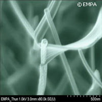
EU | Posted on July 12th, 2010The successful approach synthesises the complex and incredibly thin nanowire structures, and joins them to electrically conducting links (essentially creating an electronic circuit). The result is a culmination of work that began in 2006 under the PHODYE ('New photonic systems on a chip based on dyes for sensor applications scalable at wafer fabrication') project, which was funded EUR 1.92 million under the 'Information society technologies' (IST) Thematic area of the EU's Sixth Framework Programme (FP6).
The PHODYE project was initiated by Dr Angel Barranco from the Instituto de Ciencia de Materiales de Sevilla in Spain, who invited his former colleagues from the Swiss Federal Laboratories for Materials Testing and Research (Empa) to become involved. Empa is one of eight academic and industrial partners from four European countries (Belgium, Spain, Sweden and Switzerland) currently working on the project.
The aim is to develop a new family of sensor devices that combines dye sensor films and photonic structures. These incredibly sensitive gas sensors (made up of thin films that change colour and fluoresce on contact with certain gas molecules) could eventually be used to monitor vehicle emissions or to provide warnings of the presence of poisonous substances.
It was during their work on PHODYE that Empa's Ana Borras, Oliver Gr�ning and Pierangelo Gr�ning, and J�rgen K�ble from Omicron Nanotechnology in Germany created the unique methodology for connecting organic nanowires. The result is a step towards the manufacture of cheaper and more flexible sensors, transistors, diodes, and other components, ranging from the micro all the way to the nano scale.
The physicists developed a new vacuum deposition process for synthesising organic nanowires and discovered how to manufacture nanowires with largely varying characteristics by appropriately selecting the starting molecule and the experimental conditions. Their method is particularly unusual and surprising because it has generated a perfectly monocrystalline structure by precisely controlling the substrate temperature, molecule flow and substrate treatment.
The team soon discovered that the new process was not only able to provide nanowires for the gas sensors needed under PHODYE, but it opened the door to creating complex 'nanowire electric circuits' for electronic and optoelectronic applications (e.g. solar cells).
The reason being that the range of nanowires can be used together (as required) to form networks with broadly varying properties. The secret to this lies in having decorated (using a sputter-coating process) the nanowires growing on the surface with silver nanoparticles. Thanks to these particles, more nanowires can be grown that are in electrical contact with the original wires - the foundation of an electrical circuit on the nanoscale.
Dr Gr�ning explained that the potential exists for being able to manufacture organic semiconductor materials, which are very attractive candidates for the manufacture of inexpensive, large area and flexible electronic components.
The team has presented the results of their finding in the journal Advanced Materials. The PHODYE project formally concludes in October 2010.
For more information, please visit:
Swiss Federal Laboratories for Materials Testing and Research (Empa):
www.empa.ch/plugin/template/empa/3/*/---/l=2
PHODYE www.phodye.icmse.csic.es/
Advanced Materials www3.interscience.wiley.com/journal/10008336/home
####
For more information, please click here
Copyright © CORDIS
If you have a comment, please Contact us.Issuers of news releases, not 7th Wave, Inc. or Nanotechnology Now, are solely responsible for the accuracy of the content.
Bookmark:


| Related News Press |
News and information
![]() Simulating magnetization in a Heisenberg quantum spin chain April 5th, 2024
Simulating magnetization in a Heisenberg quantum spin chain April 5th, 2024
![]() NRL charters Navy�s quantum inertial navigation path to reduce drift April 5th, 2024
NRL charters Navy�s quantum inertial navigation path to reduce drift April 5th, 2024
![]() Discovery points path to flash-like memory for storing qubits: Rice find could hasten development of nonvolatile quantum memory April 5th, 2024
Discovery points path to flash-like memory for storing qubits: Rice find could hasten development of nonvolatile quantum memory April 5th, 2024
![]() Good as gold - improving infectious disease testing with gold nanoparticles April 5th, 2024
Good as gold - improving infectious disease testing with gold nanoparticles April 5th, 2024
Thin films
![]() Utilizing palladium for addressing contact issues of buried oxide thin film transistors April 5th, 2024
Utilizing palladium for addressing contact issues of buried oxide thin film transistors April 5th, 2024
![]() Understanding the mechanism of non-uniform formation of diamond film on tools: Paving the way to a dry process with less environmental impact March 24th, 2023
Understanding the mechanism of non-uniform formation of diamond film on tools: Paving the way to a dry process with less environmental impact March 24th, 2023
![]() New study introduces the best graphite films: The work by Distinguished Professor Feng Ding at UNIST has been published in the October 2022 issue of Nature Nanotechnology November 4th, 2022
New study introduces the best graphite films: The work by Distinguished Professor Feng Ding at UNIST has been published in the October 2022 issue of Nature Nanotechnology November 4th, 2022
Possible Futures
![]() Discovery points path to flash-like memory for storing qubits: Rice find could hasten development of nonvolatile quantum memory April 5th, 2024
Discovery points path to flash-like memory for storing qubits: Rice find could hasten development of nonvolatile quantum memory April 5th, 2024
![]() With VECSELs towards the quantum internet Fraunhofer: IAF achieves record output power with VECSEL for quantum frequency converters April 5th, 2024
With VECSELs towards the quantum internet Fraunhofer: IAF achieves record output power with VECSEL for quantum frequency converters April 5th, 2024
Academic/Education
![]() Rice University launches Rice Synthetic Biology Institute to improve lives January 12th, 2024
Rice University launches Rice Synthetic Biology Institute to improve lives January 12th, 2024
![]() Multi-institution, $4.6 million NSF grant to fund nanotechnology training September 9th, 2022
Multi-institution, $4.6 million NSF grant to fund nanotechnology training September 9th, 2022
Sensors
Nanoelectronics
![]() Interdisciplinary: Rice team tackles the future of semiconductors Multiferroics could be the key to ultralow-energy computing October 6th, 2023
Interdisciplinary: Rice team tackles the future of semiconductors Multiferroics could be the key to ultralow-energy computing October 6th, 2023
![]() Key element for a scalable quantum computer: Physicists from Forschungszentrum J�lich and RWTH Aachen University demonstrate electron transport on a quantum chip September 23rd, 2022
Key element for a scalable quantum computer: Physicists from Forschungszentrum J�lich and RWTH Aachen University demonstrate electron transport on a quantum chip September 23rd, 2022
![]() Reduced power consumption in semiconductor devices September 23rd, 2022
Reduced power consumption in semiconductor devices September 23rd, 2022
![]() Atomic level deposition to extend Moore�s law and beyond July 15th, 2022
Atomic level deposition to extend Moore�s law and beyond July 15th, 2022
Announcements
![]() NRL charters Navy�s quantum inertial navigation path to reduce drift April 5th, 2024
NRL charters Navy�s quantum inertial navigation path to reduce drift April 5th, 2024
![]() Discovery points path to flash-like memory for storing qubits: Rice find could hasten development of nonvolatile quantum memory April 5th, 2024
Discovery points path to flash-like memory for storing qubits: Rice find could hasten development of nonvolatile quantum memory April 5th, 2024
Photonics/Optics/Lasers
![]() With VECSELs towards the quantum internet Fraunhofer: IAF achieves record output power with VECSEL for quantum frequency converters April 5th, 2024
With VECSELs towards the quantum internet Fraunhofer: IAF achieves record output power with VECSEL for quantum frequency converters April 5th, 2024
![]() Nanoscale CL thermometry with lanthanide-doped heavy-metal oxide in TEM March 8th, 2024
Nanoscale CL thermometry with lanthanide-doped heavy-metal oxide in TEM March 8th, 2024
![]() Optically trapped quantum droplets of light can bind together to form macroscopic complexes March 8th, 2024
Optically trapped quantum droplets of light can bind together to form macroscopic complexes March 8th, 2024
![]() HKUST researchers develop new integration technique for efficient coupling of III-V and silicon February 16th, 2024
HKUST researchers develop new integration technique for efficient coupling of III-V and silicon February 16th, 2024
Research partnerships
![]() Discovery points path to flash-like memory for storing qubits: Rice find could hasten development of nonvolatile quantum memory April 5th, 2024
Discovery points path to flash-like memory for storing qubits: Rice find could hasten development of nonvolatile quantum memory April 5th, 2024
![]() Researchers� approach may protect quantum computers from attacks March 8th, 2024
Researchers� approach may protect quantum computers from attacks March 8th, 2024
![]() 'Sudden death' of quantum fluctuations defies current theories of superconductivity: Study challenges the conventional wisdom of superconducting quantum transitions January 12th, 2024
'Sudden death' of quantum fluctuations defies current theories of superconductivity: Study challenges the conventional wisdom of superconducting quantum transitions January 12th, 2024
|
|
||
|
|
||
| The latest news from around the world, FREE | ||
|
|
||
|
|
||
| Premium Products | ||
|
|
||
|
Only the news you want to read!
Learn More |
||
|
|
||
|
Full-service, expert consulting
Learn More |
||
|
|
||