Home > Press > Nanowires for the electronics and optoelectronics of the future
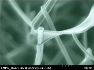 |
| Under the scanning electron microscope (SEM): palladium octaethyl-porphyrin nano-lamellae and nanowires growing on a perylene nanowire which has been sputtered with silver particles. |
Abstract:
Process for manufacturing nanoelectronic "mini-circuits" developed
Nanowires for the electronics and optoelectronics of the future
Switzerland | Posted on June 24th, 2010The tale begins with a feasibility study on the manufacture of colored fluorescing thin films for optical safety applications. An EU project on the development of novel gas sensors followed. In the meantime, Empa researchers have successfully synthesized complex organic nanowires and managed to attach them together with electrically conducting links - the first step towards the future production of electronic and optoelectronic components.
Organic semiconductors are very promising candidates as starting materials for the manufacture of cheap, large area and flexible electronic components such as transistors, diodes and sensors on a scale ranging from micro to nano. A condition for success in achieving this goal is the ability to join components together with electrically conducting links - in other words, to create an electronic circuit. Empa scientists have developed a new method which allows them to create simple networks of organic nanowires.
The origin: an EU project called �PHODYE�
When Spanish physicist Angel Barranco returned to Valencia after a three year research stint at Empa, he initiated the EU project �PHODYE� with, among others, his old Empa colleagues. The aim is to develop highly sensitive gas sensors, for monitoring road vehicle emissions, for example, or for providing laboratory staff and mine workers with an early warning of the presence of poisonous substances. The sensors are based on fluorescing thin films which change color and fluoresce on contact with certain gas molecules.
"We were thinking in terms of a sort of electronic key for security applications, which would only react to certain optical conditions," explains Empa physicist Pierangelo Groening. Necessary for this are transparent, strongly fluorescing thin films, so Groening and Barranco developed a plasma-deposition process in order to store fluorescing dye molecules such as metallo-proyphins, perylenes and phthalocyanines unmodified and at high concentrations in SiO2 or TiO2 layers.
It soon became apparent that if certain gas molecules deposited on dye particles in the thin films, then these fluoresced at different wavelengths and the thin film changed color as a result. If different dyes are used then the gases which are toxic to humans can be detected at very low concentrations.
A surprisingly wide range of uses
However, for many sensor applications it is important that the response time be as short as possible, something which is hardly possible with compact plasma dye layers. It is, on the other hand, possible with layers which have very a porous structure, resembling the nap of a nanometer-scale carpet. Scientists hope to derive further benefits from such layers because they increase the area onto which the gas molecules to be detected can adsorb, and also shorten the diffusion distances, allowing the sensor to respond faster. Physicist Ana Borras thereupon developed a new vacuum deposition process for synthesizing organic nanowires.
In the meantime the Empa researchers made progress, learning how to manufacture nanowires with very widely varying characteristics by appropriately selecting the starting molecule and the experimental conditions. Nanowires of metallo-phthalocyanine molecules have diameters of a mere 10 to 50 nanometers and a length of up to 100 microns. What is unusual and unexpected about the new method is that by exactly controlling the substrate temperature, molecule flow and substrate treatment, the organic nanowires develop a previously unattained, perfectly monocrystalline structure.
Immediately after the first studies were made with the electron microscope it was clear to Groening that the new process could not only provide nanowires for the gas sensors but also make it possible to create complex "nanowire electric circuits" for electronic and optoelectronic applications such as solar cells, transistors and diodes. This is because the different types of nanowires can be combined as required to form networks with widely varying properties, as Groening and coworkers report in the scientific journal Advanced Materials and elsewhere.
The trick to achieving this lies in a second step in which the nanowires growing on the surface are "decorated" with silver nanoparticles by a sputter-coating process. A target, in this case a piece of solid silver, is bombarded with energetic ions, knocking off silver atoms which enter the gas phase and are deposited onto the nanowires. In a final step, the Empa team now grow more nanowires which, thanks to the silver particles, are in electrical contact with the original wires - the basis of an electrical circuit on the nanometer scale.
The first step from microelectronics to nanoelectronics
The first electrical conductivity measurements, made with the help of a four-tip scanning tunnel microscope in ultra high vacuum, exceeded the most optimistic expectations - the material is of an unusually high quality. "This opens up the possibility of soon being able to manufacture organic semiconductor materials," says Groening confidently. "And that, too, using a simple and economic process." In the meantime the researchers have successfully synthesized increasingly more complex structures of nanowires, and managed to link these together using a good deal of skill and a sure touch.
Take, for example, nanowires consisting of sections made with different starting molecules. If these molecules can transport either only positive or only negative charges, then a diode is created which allows current to flow in one direction alone. Groening speculates that it is quite possible that one day components for nanolectronics and nanophotonics will be made using this technique.
Reference
A. Borras, O. Groening, J. Koeble, P. Groening: Organic Nanowires: Connecting Organic Nanowires, Advanced Materials, vol. 21, issue 47, pp. 4816 - 4819; DOI: 10.1002/adma.200901724
####
About Empa
Empa is an interdisciplinary research and services institution for material sciences and technology development within the ETH Domain. Empa�s research and development activities are oriented to meeting the requirements of industry and the needs of our society, and link together applications-oriented research and the practical implementation of new ideas, science and industry, and science and society.
For more information, please click here
Contacts:
Dr. Pierangelo Gr�ning
Empa,
Tel. +41 44 823 40 04
+41 33 228 52 15
Editor / Media contact
Dr. Michael Hagmann
Empa, Communication Dept.
Tel. +41 44 823 45 92
Copyright © Empa
If you have a comment, please Contact us.Issuers of news releases, not 7th Wave, Inc. or Nanotechnology Now, are solely responsible for the accuracy of the content.
Bookmark:


| Related News Press |
News and information
![]() Simulating magnetization in a Heisenberg quantum spin chain April 5th, 2024
Simulating magnetization in a Heisenberg quantum spin chain April 5th, 2024
![]() NRL charters Navy�s quantum inertial navigation path to reduce drift April 5th, 2024
NRL charters Navy�s quantum inertial navigation path to reduce drift April 5th, 2024
![]() Discovery points path to flash-like memory for storing qubits: Rice find could hasten development of nonvolatile quantum memory April 5th, 2024
Discovery points path to flash-like memory for storing qubits: Rice find could hasten development of nonvolatile quantum memory April 5th, 2024
Chip Technology
![]() Discovery points path to flash-like memory for storing qubits: Rice find could hasten development of nonvolatile quantum memory April 5th, 2024
Discovery points path to flash-like memory for storing qubits: Rice find could hasten development of nonvolatile quantum memory April 5th, 2024
![]() Utilizing palladium for addressing contact issues of buried oxide thin film transistors April 5th, 2024
Utilizing palladium for addressing contact issues of buried oxide thin film transistors April 5th, 2024
![]() HKUST researchers develop new integration technique for efficient coupling of III-V and silicon February 16th, 2024
HKUST researchers develop new integration technique for efficient coupling of III-V and silicon February 16th, 2024
Sensors
Nanoelectronics
![]() Interdisciplinary: Rice team tackles the future of semiconductors Multiferroics could be the key to ultralow-energy computing October 6th, 2023
Interdisciplinary: Rice team tackles the future of semiconductors Multiferroics could be the key to ultralow-energy computing October 6th, 2023
![]() Key element for a scalable quantum computer: Physicists from Forschungszentrum J�lich and RWTH Aachen University demonstrate electron transport on a quantum chip September 23rd, 2022
Key element for a scalable quantum computer: Physicists from Forschungszentrum J�lich and RWTH Aachen University demonstrate electron transport on a quantum chip September 23rd, 2022
![]() Reduced power consumption in semiconductor devices September 23rd, 2022
Reduced power consumption in semiconductor devices September 23rd, 2022
![]() Atomic level deposition to extend Moore�s law and beyond July 15th, 2022
Atomic level deposition to extend Moore�s law and beyond July 15th, 2022
Announcements
![]() NRL charters Navy�s quantum inertial navigation path to reduce drift April 5th, 2024
NRL charters Navy�s quantum inertial navigation path to reduce drift April 5th, 2024
![]() Discovery points path to flash-like memory for storing qubits: Rice find could hasten development of nonvolatile quantum memory April 5th, 2024
Discovery points path to flash-like memory for storing qubits: Rice find could hasten development of nonvolatile quantum memory April 5th, 2024
Photonics/Optics/Lasers
![]() With VECSELs towards the quantum internet Fraunhofer: IAF achieves record output power with VECSEL for quantum frequency converters April 5th, 2024
With VECSELs towards the quantum internet Fraunhofer: IAF achieves record output power with VECSEL for quantum frequency converters April 5th, 2024
![]() Nanoscale CL thermometry with lanthanide-doped heavy-metal oxide in TEM March 8th, 2024
Nanoscale CL thermometry with lanthanide-doped heavy-metal oxide in TEM March 8th, 2024
![]() Optically trapped quantum droplets of light can bind together to form macroscopic complexes March 8th, 2024
Optically trapped quantum droplets of light can bind together to form macroscopic complexes March 8th, 2024
![]() HKUST researchers develop new integration technique for efficient coupling of III-V and silicon February 16th, 2024
HKUST researchers develop new integration technique for efficient coupling of III-V and silicon February 16th, 2024
Solar/Photovoltaic
![]() Development of zinc oxide nanopagoda array photoelectrode: photoelectrochemical water-splitting hydrogen production January 12th, 2024
Development of zinc oxide nanopagoda array photoelectrode: photoelectrochemical water-splitting hydrogen production January 12th, 2024
![]() Shedding light on unique conduction mechanisms in a new type of perovskite oxide November 17th, 2023
Shedding light on unique conduction mechanisms in a new type of perovskite oxide November 17th, 2023
![]() Inverted perovskite solar cell breaks 25% efficiency record: Researchers improve cell efficiency using a combination of molecules to address different November 17th, 2023
Inverted perovskite solar cell breaks 25% efficiency record: Researchers improve cell efficiency using a combination of molecules to address different November 17th, 2023
![]() Charged �molecular beasts� the basis for new compounds: Researchers at Leipzig University use �aggressive� fragments of molecular ions for chemical synthesis November 3rd, 2023
Charged �molecular beasts� the basis for new compounds: Researchers at Leipzig University use �aggressive� fragments of molecular ions for chemical synthesis November 3rd, 2023
|
|
||
|
|
||
| The latest news from around the world, FREE | ||
|
|
||
|
|
||
| Premium Products | ||
|
|
||
|
Only the news you want to read!
Learn More |
||
|
|
||
|
Full-service, expert consulting
Learn More |
||
|
|
||