Home > Press > Light can induce twisting in semiconductor nanoribbons
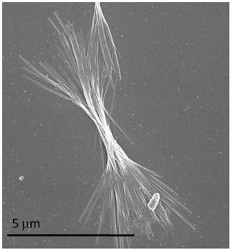 |
| Figure 2. Straight nanoribbons formed in complete darkness. |
Abstract:
A novel approach using ambient-light irradiation can produce twisted nanostructures of variable pitch length with many potential applications.
By Sudhanshu Srivastava and Nicholas A. Kotov
Light can induce twisting in semiconductor nanoribbons
Bellingham, WA | Posted on June 23rd, 2010Self-organization of nanoparticles (NPs) can create advanced architectures such as nanowires (NWs), nanosheets (NSes), nanotubes, and nanoplates. They have many possible applications in electronic-device development, biomedicine, and other areas. Different mechanisms and routes have been reported that use noncovalent interactions between NPs to create these morphologies. An interesting topic to investigate regarding their assembly is the way that changes in physical conditions, such as ambient light, can affect their overall structural shape.
We have investigated self-assembly of cadmium telluride (CdTe) NPs under controlled conditions of visible-light irradiation, producing helically twisted nanoribbons (TRs)1 with pitch lengths ranging from 1500 to 250nm under varying degrees of illumination. In contrast, we did not observe any twisting when the ribbons were assembled in complete darkness. Although light is known to affect matter, the use of ambient-light illumination to twist or bend wires by a few nanometers has not been reported before.
The dipolar interactions involved in the self-assembly of CdTe NPs can create 1D NWs2 and 2D NSs.3 Using the same concept, we prepared an aqueous solution of CdTe NPs with thioglycolic acid (TGA) as a capping agent. We used a Cd2+/TGA ratio close to unity instead of the typical value of 2.4 used for 1D NW formation. The lower amount of TGA is expected to reduce the local concentration on the tetrahedral corners of NPs and increase the dipole of the particles.
We first precipitated CdTe NPs in methanol and centrifuged them. They were then redispersed in water at pH 9 (pH: Measure of acidity or basicity of a solution). The orange color of the initial NP solution turned to dark green in three days in the presence of ambient light. We analyzed the samples under scanning-electron microscopy (SEM) and transmission-electron microscopy (TEM) and found that TRs had formed.1 The TRs were 1 to 2�m in length, with a helical pitch length of ~400nm (see Figure 1). We examined the direction of helicity for some 100 TRs and observed a racemic distribution of left- and right-handed ribbons. Under high-resolution TEM (HRTEM), the TRs showed a polycrystalline structure composed of both CdTe and cadmium sulfide (CdS) NPs. Because less TGA was used in the fabrication of the CdTe NPs, the particles were more exposed to Te oxidation. In this process, Te2− is oxidized and the excess of Cd2+ present in the particles reacts with the remaining S2− resulting from TGA decomposition to form CdS. This explains the composition of the resulting TRs.
Interestingly, the same procedure, when carried out in complete darkness, showed the same polycrystalline structure composed of CdTe/CdS NPs, but with no twisting (straight ribbons): see Figure 2. Because both CdTe and CdS are sensitive to light, the twisting is believed to be related to the exposure to ambient light.
To further investigate the effect of light illumination on the assembly of CdTe NPs into TRs, we exposed the solution described above to various levels of light illumination. The resulting TRs showed a sequential alteration in pitch length from 250 to 1500nm with increasing illumination. HRTEM observations showed that all TRs exhibited the same polycrystalline structure composed of CdTe/CdS NPs. The results clearly indicate the importance of ambient light. The wires prepared in the dark were also wider than the TRs prepared under ambient light.
The intermediate stages of sample preparation also supported the suggestion that photo-oxidation caused the twisted structures. We found unusual shapes (such as ellipsoids, dumbbell shapes, and bunches of ribbons) as intermediate stages and TRs finally emerged from these multiparticle assemblies. To further confirm that the pitch length of the TRs is controlled by ambient light, we also examined the duration of the illumination rather than its intensity. The CdTe samples were initially kept in complete darkness to form straight ribbons and then introduced to irradiation with ambient light for one day. The results showed a sequential change in pitch length from straight to ~600 and 400nm after 12 and 24hr, respectively, under ambient light. Theoretical calculations and simulations revealed that the resulting geometry and dimensionality are also controlled by electrostatic attraction and repulsion in the NP assemblies.
TRs with variable pitch length provide a new shape for use in nanotechnology. Nanoscale twisted propellers inspired by nature mimic the alpha-helical structures found in biomolecules such as proteins and DNA. Helical TRs similar to biomolecules could thus be used to control drug delivery as well as in microfluidic systems used in experiments to simulate the body. This newly discovered twisting effect could also be applied to create variable micro-electromechanical systems that are controlled by visible light. Similarly, the TRs could be used in lithography technologies and in designing microchips. Semiconductor materials can be applied as superchiral structures, which may have smart applications in the field of negative-refractive-index materials. We are currently investigating methods to construct chiral structures twisted in one direction for application as metamaterials. To further use this morphology for metamaterials with negative refractive index, we are also investigating new procedures to use them as templates for creating metallic wires with a similar twisted morphology.
Sudhanshu Srivastava
University of Michigan
Ann Arbor, MI
Sudhanshu Srivastava works as a research fellow with Nicholas Kotov. His research focuses on the spontaneous assembly of nanoparticles for construction of nanowires, nanoribbons, and other advanced architectures. He is also investigating exponential layer-by-layer assembly for loading and unloading of nanomaterials.
Nicholas Kotov
Departments of Chemical Engineering, Materials Science, and Biomedical Engineering
University of Michigan
Ann Arbor, MI
Nicholas Kotov is a professor. His research interests include nanocolloids, their assembled structures, layer-by-layer assembly, ultrastrong materials from carbon nanotubes and clays, nanomaterials for energy storage, interfacing neural tissues with nanomaterials, and diagnostics with nanoparticles.
References:
1. S. Srivastava, A. Santos, K. Critchley, K. S. Kim, P. Podsiadlo, K. Sun, J. Lee, C. Xu, G. D. Lilly, S. C. Glotzer, N. A. Kotov, Light-controlled self-assembly of semiconductor nanoparticles into twisted ribbons, Science 327, pp. 1355, 2010.
2. Z. Tang, N. A. Kotov, M. Giersig, Spontaneous organization of single CdTe nanoparticles into luminescent nanowires, Science 297, pp. 237, 2002.
3. Z. Tang, Z. Zhang, Y. Wang, S. C. Glotzer, N. A. Kotov, Self-assembly of CdTe nanocrystals into free-floating sheets, Science 314, pp. 274, 2006.
####
About International Society for Optical Engineering
SPIE is the international society for optics and photonics founded in 1955 to advance light-based technologies. Serving more than 177,000 constituents from 168 countries, the Society advances emerging technologies through interdisciplinary information exchange, continuing education, publications, patent precedent, and career and professional growth.
SPIE annually organizes and sponsors approximately 25 major technical forums, exhibitions, and education programs in North America, Europe, Asia, and the South Pacific.
In 2009, the Society provided more than $2 million in support of scholarships, grants, and other education programs around the world.
For more information, please click here
Copyright © International Society for Optical Engineering
If you have a comment, please Contact us.Issuers of news releases, not 7th Wave, Inc. or Nanotechnology Now, are solely responsible for the accuracy of the content.
Bookmark:


| Related News Press |
News and information
![]() Simulating magnetization in a Heisenberg quantum spin chain April 5th, 2024
Simulating magnetization in a Heisenberg quantum spin chain April 5th, 2024
![]() NRL charters Navy�s quantum inertial navigation path to reduce drift April 5th, 2024
NRL charters Navy�s quantum inertial navigation path to reduce drift April 5th, 2024
![]() Discovery points path to flash-like memory for storing qubits: Rice find could hasten development of nonvolatile quantum memory April 5th, 2024
Discovery points path to flash-like memory for storing qubits: Rice find could hasten development of nonvolatile quantum memory April 5th, 2024
Possible Futures
![]() Discovery points path to flash-like memory for storing qubits: Rice find could hasten development of nonvolatile quantum memory April 5th, 2024
Discovery points path to flash-like memory for storing qubits: Rice find could hasten development of nonvolatile quantum memory April 5th, 2024
![]() With VECSELs towards the quantum internet Fraunhofer: IAF achieves record output power with VECSEL for quantum frequency converters April 5th, 2024
With VECSELs towards the quantum internet Fraunhofer: IAF achieves record output power with VECSEL for quantum frequency converters April 5th, 2024
Self Assembly
![]() Liquid crystal templated chiral nanomaterials October 14th, 2022
Liquid crystal templated chiral nanomaterials October 14th, 2022
![]() Nanoclusters self-organize into centimeter-scale hierarchical assemblies April 22nd, 2022
Nanoclusters self-organize into centimeter-scale hierarchical assemblies April 22nd, 2022
![]() Atom by atom: building precise smaller nanoparticles with templates March 4th, 2022
Atom by atom: building precise smaller nanoparticles with templates March 4th, 2022
![]() Nanostructures get complex with electron equivalents: Nanoparticles of two different sizes break away from symmetrical designs January 14th, 2022
Nanostructures get complex with electron equivalents: Nanoparticles of two different sizes break away from symmetrical designs January 14th, 2022
Nanotubes/Buckyballs/Fullerenes/Nanorods/Nanostrings
![]() Tests find no free-standing nanotubes released from tire tread wear September 8th, 2023
Tests find no free-standing nanotubes released from tire tread wear September 8th, 2023
![]() Detection of bacteria and viruses with fluorescent nanotubes July 21st, 2023
Detection of bacteria and viruses with fluorescent nanotubes July 21st, 2023
Nanomedicine
![]() New micromaterial releases nanoparticles that selectively destroy cancer cells April 5th, 2024
New micromaterial releases nanoparticles that selectively destroy cancer cells April 5th, 2024
![]() Good as gold - improving infectious disease testing with gold nanoparticles April 5th, 2024
Good as gold - improving infectious disease testing with gold nanoparticles April 5th, 2024
![]() Researchers develop artificial building blocks of life March 8th, 2024
Researchers develop artificial building blocks of life March 8th, 2024
Discoveries
![]() Chemical reactions can scramble quantum information as well as black holes April 5th, 2024
Chemical reactions can scramble quantum information as well as black holes April 5th, 2024
![]() New micromaterial releases nanoparticles that selectively destroy cancer cells April 5th, 2024
New micromaterial releases nanoparticles that selectively destroy cancer cells April 5th, 2024
![]() Utilizing palladium for addressing contact issues of buried oxide thin film transistors April 5th, 2024
Utilizing palladium for addressing contact issues of buried oxide thin film transistors April 5th, 2024
Announcements
![]() NRL charters Navy�s quantum inertial navigation path to reduce drift April 5th, 2024
NRL charters Navy�s quantum inertial navigation path to reduce drift April 5th, 2024
![]() Discovery points path to flash-like memory for storing qubits: Rice find could hasten development of nonvolatile quantum memory April 5th, 2024
Discovery points path to flash-like memory for storing qubits: Rice find could hasten development of nonvolatile quantum memory April 5th, 2024
Nanobiotechnology
![]() New micromaterial releases nanoparticles that selectively destroy cancer cells April 5th, 2024
New micromaterial releases nanoparticles that selectively destroy cancer cells April 5th, 2024
![]() Good as gold - improving infectious disease testing with gold nanoparticles April 5th, 2024
Good as gold - improving infectious disease testing with gold nanoparticles April 5th, 2024
![]() Researchers develop artificial building blocks of life March 8th, 2024
Researchers develop artificial building blocks of life March 8th, 2024
|
|
||
|
|
||
| The latest news from around the world, FREE | ||
|
|
||
|
|
||
| Premium Products | ||
|
|
||
|
Only the news you want to read!
Learn More |
||
|
|
||
|
Full-service, expert consulting
Learn More |
||
|
|
||