Home > Press > Bayer opens Functional Films Research Centre in Singapore, its first in Asia Pacific
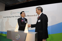 |
| Mr. Patrick Thomas, CEO of Bayer MaterialScience, and Dr. Beh Swan Gin, Managing Director of the Singapore Economic Development Board, leading the official opening of the new Functional Films Centre in Singapore |
Abstract:
Initial investment of SGD 12 million (€ 7 million) to develop technological applications for future electronics
Bayer opens Functional Films Research Centre in Singapore, its first in Asia Pacific
Singapore | Posted on June 22nd, 2010Key executives of Bayer MaterialScience and the Singapore Economic Development Board officially opened today the company's new Functional Films Research Centre. The full-scale facility for upstream research will focus on coated high-tech films and nanotechnology to meet the ever-evolving and growing demand of the electronics market in Asia Pacific.
The centre represents an initial investment of approximately SGD 12 million (€ 7 million) with a further provision for broadening its capabilities in subsequent years. Using self-developed material technologies, Bayer MaterialScience will pursue joint projects with collaboration partners to create advanced technological breakthroughs in electronics. These include functional films that can be applied to flexible screens and three-dimensional displays, and nanomaterials like conductive inks used in printed electronics or energy-efficient lighting technologies.
Speaking at the launch of the research centre, Mr. Patrick Thomas, CEO of Bayer MaterialScience AG (Germany) said, "The opening of this facility is a clear indication of our continued commitment to Singapore and its unique position as an economic and business hub for the Asian region. This confidence is underpinned by the fact that demand continues to grow for new and innovative film-based products. Much of the research and development for these new materials will be undertaken at this new centre. I would like to pay tribute to the government of Singapore and the Economic Development Board for its support in establishing this R&D facility."
"We are delighted that Singapore will be the location of Bayer MaterialScience's first Functional Films Research Centre outside of Germany. This reaffirms Singapore's attractiveness as a strategic base for research & development to meet the fast evolving market needs in Asia and globally," remarked Dr Beh Swan Gin, Managing Director of Singapore Economic Development Board, at the official opening.
For Bayer MaterialScience, this is the first research centre of its kind in Asia Pacific and outside Germany. "Since 2008, Functional Films of Bayer MaterialScience has been building up research resources and networks in the Asia Pacific region for customer-oriented developments, primarily in Japan, Korea and Taiwan," said Mr. Marcus Yim, Managing Director of Bayer South East Asia. "By collaborating with a network of research organisations and business partners in Singapore and the whole of Asia Pacific, we will put to use the innovative ideas to fast-track products for tomorrow's markets like automotives, electronics and displays," he continued.
The Functional Films Research Centre presently houses about 30 researchers and staff.
Forward-Looking Statements
This release may contain forward-looking statements based on current assumptions and forecasts made by Bayer Group or subgroup management. Various known and unknown risks, uncertainties and other factors could lead to material differences between the actual future results, financial situation, development or performance of the company and the estimates given here. These factors include those discussed in Bayer's public reports which are available on the Bayer website at www.bayer.com. The company assumes no liability whatsoever to update these forward-looking statements or to conform them to future events or developments.
####
About Bayer MaterialScience
With 2009 sales of EUR 7.5 billion, Bayer MaterialScience is among the world’s largest polymer companies. Business activities are focused on the manufacture of high-tech polymer materials and the development of innovative solutions for products used in many areas of daily life. The main segments served are the automotive, electrical and electronics, construction and sports and leisure industries. Bayer MaterialScience has 30 production sites around the globe and employed approximately 14,300 people at the end of 2009. Bayer MaterialScience is a Bayer Group company.
Find more information at www.bayermaterialscience.com and www.functional-films.com.
For more information, please click here
Copyright © Bayer MaterialScience
If you have a comment, please Contact us.Issuers of news releases, not 7th Wave, Inc. or Nanotechnology Now, are solely responsible for the accuracy of the content.
Bookmark:


| Related News Press |
News and information
![]() Simulating magnetization in a Heisenberg quantum spin chain April 5th, 2024
Simulating magnetization in a Heisenberg quantum spin chain April 5th, 2024
![]() NRL charters Navy’s quantum inertial navigation path to reduce drift April 5th, 2024
NRL charters Navy’s quantum inertial navigation path to reduce drift April 5th, 2024
![]() Discovery points path to flash-like memory for storing qubits: Rice find could hasten development of nonvolatile quantum memory April 5th, 2024
Discovery points path to flash-like memory for storing qubits: Rice find could hasten development of nonvolatile quantum memory April 5th, 2024
![]() Good as gold - improving infectious disease testing with gold nanoparticles April 5th, 2024
Good as gold - improving infectious disease testing with gold nanoparticles April 5th, 2024
Display technology/LEDs/SS Lighting/OLEDs
![]() Utilizing palladium for addressing contact issues of buried oxide thin film transistors April 5th, 2024
Utilizing palladium for addressing contact issues of buried oxide thin film transistors April 5th, 2024
![]() Light guide plate based on perovskite nanocomposites November 3rd, 2023
Light guide plate based on perovskite nanocomposites November 3rd, 2023
![]() Simple ballpoint pen can write custom LEDs August 11th, 2023
Simple ballpoint pen can write custom LEDs August 11th, 2023
Thin films
![]() Utilizing palladium for addressing contact issues of buried oxide thin film transistors April 5th, 2024
Utilizing palladium for addressing contact issues of buried oxide thin film transistors April 5th, 2024
![]() Thin-film, high-frequency antenna array offers new flexibility for wireless communications November 5th, 2021
Thin-film, high-frequency antenna array offers new flexibility for wireless communications November 5th, 2021
![]() Leibniz Prize winner Professor Dr. Oliver G. Schmidt moves to Chemnitz University of Technology: President Professor Dr. Gerd Strohmeier refers to an 'absolute top transfer' September 10th, 2021
Leibniz Prize winner Professor Dr. Oliver G. Schmidt moves to Chemnitz University of Technology: President Professor Dr. Gerd Strohmeier refers to an 'absolute top transfer' September 10th, 2021
Openings/New facilities/Groundbreaking/Expansion
![]() OCSiAl expands its graphene nanotube production capacities to Europe June 17th, 2022
OCSiAl expands its graphene nanotube production capacities to Europe June 17th, 2022
![]() GLOBALFOUNDRIES Moves Corporate Headquarters to its Most Advanced Semiconductor Manufacturing Facility in New York April 27th, 2021
GLOBALFOUNDRIES Moves Corporate Headquarters to its Most Advanced Semiconductor Manufacturing Facility in New York April 27th, 2021
Jobs
![]() Could quantum technology be New Mexico’s next economic boon? Quantum New Mexico Coalition aims to establish state as national hub April 1st, 2022
Could quantum technology be New Mexico’s next economic boon? Quantum New Mexico Coalition aims to establish state as national hub April 1st, 2022
![]() SEMI Partners with GLOBALFOUNDRIES to Offer Apprenticeship Program Aimed at Building the Electronics Talent Pipeline August 11th, 2020
SEMI Partners with GLOBALFOUNDRIES to Offer Apprenticeship Program Aimed at Building the Electronics Talent Pipeline August 11th, 2020
![]() Arrowhead Pharmaceuticals Reports Inducement Grants under NASDAQ Marketplace Rule 5635(c)(4) March 29th, 2019
Arrowhead Pharmaceuticals Reports Inducement Grants under NASDAQ Marketplace Rule 5635(c)(4) March 29th, 2019
Govt.-Legislation/Regulation/Funding/Policy
![]() NRL charters Navy’s quantum inertial navigation path to reduce drift April 5th, 2024
NRL charters Navy’s quantum inertial navigation path to reduce drift April 5th, 2024
![]() Discovery points path to flash-like memory for storing qubits: Rice find could hasten development of nonvolatile quantum memory April 5th, 2024
Discovery points path to flash-like memory for storing qubits: Rice find could hasten development of nonvolatile quantum memory April 5th, 2024
![]() Chemical reactions can scramble quantum information as well as black holes April 5th, 2024
Chemical reactions can scramble quantum information as well as black holes April 5th, 2024
Nanoelectronics
![]() Interdisciplinary: Rice team tackles the future of semiconductors Multiferroics could be the key to ultralow-energy computing October 6th, 2023
Interdisciplinary: Rice team tackles the future of semiconductors Multiferroics could be the key to ultralow-energy computing October 6th, 2023
![]() Key element for a scalable quantum computer: Physicists from Forschungszentrum Jülich and RWTH Aachen University demonstrate electron transport on a quantum chip September 23rd, 2022
Key element for a scalable quantum computer: Physicists from Forschungszentrum Jülich and RWTH Aachen University demonstrate electron transport on a quantum chip September 23rd, 2022
![]() Reduced power consumption in semiconductor devices September 23rd, 2022
Reduced power consumption in semiconductor devices September 23rd, 2022
![]() Atomic level deposition to extend Moore’s law and beyond July 15th, 2022
Atomic level deposition to extend Moore’s law and beyond July 15th, 2022
Materials/Metamaterials/Magnetoresistance
![]() Nanoscale CL thermometry with lanthanide-doped heavy-metal oxide in TEM March 8th, 2024
Nanoscale CL thermometry with lanthanide-doped heavy-metal oxide in TEM March 8th, 2024
![]() Focused ion beam technology: A single tool for a wide range of applications January 12th, 2024
Focused ion beam technology: A single tool for a wide range of applications January 12th, 2024
Announcements
![]() NRL charters Navy’s quantum inertial navigation path to reduce drift April 5th, 2024
NRL charters Navy’s quantum inertial navigation path to reduce drift April 5th, 2024
![]() Discovery points path to flash-like memory for storing qubits: Rice find could hasten development of nonvolatile quantum memory April 5th, 2024
Discovery points path to flash-like memory for storing qubits: Rice find could hasten development of nonvolatile quantum memory April 5th, 2024
Energy
![]() Development of zinc oxide nanopagoda array photoelectrode: photoelectrochemical water-splitting hydrogen production January 12th, 2024
Development of zinc oxide nanopagoda array photoelectrode: photoelectrochemical water-splitting hydrogen production January 12th, 2024
![]() Shedding light on unique conduction mechanisms in a new type of perovskite oxide November 17th, 2023
Shedding light on unique conduction mechanisms in a new type of perovskite oxide November 17th, 2023
![]() Inverted perovskite solar cell breaks 25% efficiency record: Researchers improve cell efficiency using a combination of molecules to address different November 17th, 2023
Inverted perovskite solar cell breaks 25% efficiency record: Researchers improve cell efficiency using a combination of molecules to address different November 17th, 2023
![]() The efficient perovskite cells with a structured anti-reflective layer – another step towards commercialization on a wider scale October 6th, 2023
The efficient perovskite cells with a structured anti-reflective layer – another step towards commercialization on a wider scale October 6th, 2023
Automotive/Transportation
![]() Researchers’ approach may protect quantum computers from attacks March 8th, 2024
Researchers’ approach may protect quantum computers from attacks March 8th, 2024
![]() Tests find no free-standing nanotubes released from tire tread wear September 8th, 2023
Tests find no free-standing nanotubes released from tire tread wear September 8th, 2023
Alliances/Trade associations/Partnerships/Distributorships
![]() Chicago Quantum Exchange welcomes six new partners highlighting quantum technology solutions, from Chicago and beyond September 23rd, 2022
Chicago Quantum Exchange welcomes six new partners highlighting quantum technology solutions, from Chicago and beyond September 23rd, 2022
![]() University of Illinois Chicago joins Brookhaven Lab's Quantum Center June 10th, 2022
University of Illinois Chicago joins Brookhaven Lab's Quantum Center June 10th, 2022
|
|
||
|
|
||
| The latest news from around the world, FREE | ||
|
|
||
|
|
||
| Premium Products | ||
|
|
||
|
Only the news you want to read!
Learn More |
||
|
|
||
|
Full-service, expert consulting
Learn More |
||
|
|
||