Home > Press > Imec demonstrates integrated electrical sources of surface plasmons
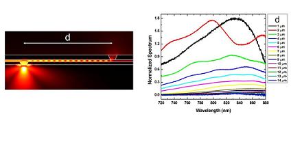 |
| Simulated (left) and experimental (right) coupling of the light emitted by a light-emitting diode (LED) into a MIM waveguide. The left figure shows the electric field profile that results of the coupling of a dipole emitter placed near a subwavelength slit in the bottom layer of the MIM waveguide. The emitted light couples efficiently to the plasmon waveguide mode and results in a standing wave pattern between two slits in the waveguide. This is also measured experimentally, as shown in the spectrally resolved output in the right figure for different lengths between the slits. |
Abstract:
Imec has fabricated electrical sources of surface plasmons, based on integrating light emitting diodes with metal-insulator-metal (MIM) waveguides. These sources, together with earlier work demonstrating plasmon detectors, are a prerequisite for making an interface between electronics and plasmonic circuits. This will lead the way to fully integrated plasmonic biosensing.
Imec demonstrates integrated electrical sources of surface plasmons
Belgium | Posted on June 22nd, 2010Metal-based nanophotonics (plasmonics) is a field concerned with manipulating and focusing light on nanoscale structures that are much smaller than conventional optic components. Plasmonic technology, today still in an experimental stage, has the potential to be used in future applications such as nanoscale optical interconnects for high performance computer chips, highly efficient thin-film solar cells, and extremely sensitive (bio)molecular sensors.
On the nanoscale, incoming light results in surface plasmon polaritons (SPPs), charge density oscillations at metal-dielectric interfaces. These have proven to be excellent markers for biochemical events, because they strongly enhance the local field near metal surfaces or nanostructures, and thus also the specific change induced by the presence of even ultrasmall quantities of biomolecules. Such a detection technique based on surface plasmon resonance (SPR) on thin gold films has already been successfully commercialized. But this technique still uses large external light sources and detectors.
The state of the art in plasmonic waveguides has already been pushed forward substantially during the past years, demonstrating both plasmon propagation in low-loss long-range plasmon waveguides and highly confined plasmon propagation in e.g. metal-dielectric-metal waveguides. However, in order to incorporate such waveguides in realistic integrated circuits, they need to interface with fast and efficient electronics. But to do so, we'd need integrated electrical SPP sources and SPP detectors.
In recent publications in Nano Letters (De Vlaminck, Van Dorpe et al, 2007) and Nature Photonics (Neutens, Van Dorpe et al, 2009), imec has demonstrated the feasibility of efficient integrated detectors of surface plasmons. We have now extended this to integrated electrical sources of surface plasmons based on integrating light emitting diodes with metal-insulator-metal (MIM) waveguides. The strong measured polarization dependence, the experimentally obtained influence of the waveguide length, the measured spectral response are all in line with theoretical expectations. Also surface plasmon polariton interference inside the waveguide is experimentally observed, which allowed us to reliably extract information about the wavelength and confinement of the propagating plasmons (illustrated in the figure). The realization of this building block completes the toolset that is needed to construct truly integrated electrically driven plasmonic circuits and hence paves the way for the integration of nanoscale plasmonic circuitry and integrated plasmonic biosensing.
This work has been published in the highly ranked journal Nano Letters: Neutens et al, Nano Lett. 2010, 10, 1429-1432.
####
About imec
Imec is Europe�s largest independent research center in nanoelectronics and nano-technology. Its staff of more than 1,750 people includes over 550 industrial residents and guest researchers. Imec�s research is applied in better healthcare, smart electronics, sustainable energy, and safer transport.
For more information, please click here
Contacts:
Kapeldreef 75
B-3001 Leuven
Belgium
Phone: +32 16 28 12 11
Fax: +32 16 22 94 00
Copyright © imec
If you have a comment, please Contact us.Issuers of news releases, not 7th Wave, Inc. or Nanotechnology Now, are solely responsible for the accuracy of the content.
Bookmark:


| Related News Press |
News and information
![]() Simulating magnetization in a Heisenberg quantum spin chain April 5th, 2024
Simulating magnetization in a Heisenberg quantum spin chain April 5th, 2024
![]() NRL charters Navy�s quantum inertial navigation path to reduce drift April 5th, 2024
NRL charters Navy�s quantum inertial navigation path to reduce drift April 5th, 2024
![]() Discovery points path to flash-like memory for storing qubits: Rice find could hasten development of nonvolatile quantum memory April 5th, 2024
Discovery points path to flash-like memory for storing qubits: Rice find could hasten development of nonvolatile quantum memory April 5th, 2024
![]() Good as gold - improving infectious disease testing with gold nanoparticles April 5th, 2024
Good as gold - improving infectious disease testing with gold nanoparticles April 5th, 2024
Display technology/LEDs/SS Lighting/OLEDs
![]() Utilizing palladium for addressing contact issues of buried oxide thin film transistors April 5th, 2024
Utilizing palladium for addressing contact issues of buried oxide thin film transistors April 5th, 2024
![]() Light guide plate based on perovskite nanocomposites November 3rd, 2023
Light guide plate based on perovskite nanocomposites November 3rd, 2023
![]() Simple ballpoint pen can write custom LEDs August 11th, 2023
Simple ballpoint pen can write custom LEDs August 11th, 2023
Possible Futures
![]() Discovery points path to flash-like memory for storing qubits: Rice find could hasten development of nonvolatile quantum memory April 5th, 2024
Discovery points path to flash-like memory for storing qubits: Rice find could hasten development of nonvolatile quantum memory April 5th, 2024
![]() With VECSELs towards the quantum internet Fraunhofer: IAF achieves record output power with VECSEL for quantum frequency converters April 5th, 2024
With VECSELs towards the quantum internet Fraunhofer: IAF achieves record output power with VECSEL for quantum frequency converters April 5th, 2024
Chip Technology
![]() Discovery points path to flash-like memory for storing qubits: Rice find could hasten development of nonvolatile quantum memory April 5th, 2024
Discovery points path to flash-like memory for storing qubits: Rice find could hasten development of nonvolatile quantum memory April 5th, 2024
![]() Utilizing palladium for addressing contact issues of buried oxide thin film transistors April 5th, 2024
Utilizing palladium for addressing contact issues of buried oxide thin film transistors April 5th, 2024
![]() HKUST researchers develop new integration technique for efficient coupling of III-V and silicon February 16th, 2024
HKUST researchers develop new integration technique for efficient coupling of III-V and silicon February 16th, 2024
Sensors
Nanoelectronics
![]() Interdisciplinary: Rice team tackles the future of semiconductors Multiferroics could be the key to ultralow-energy computing October 6th, 2023
Interdisciplinary: Rice team tackles the future of semiconductors Multiferroics could be the key to ultralow-energy computing October 6th, 2023
![]() Key element for a scalable quantum computer: Physicists from Forschungszentrum J�lich and RWTH Aachen University demonstrate electron transport on a quantum chip September 23rd, 2022
Key element for a scalable quantum computer: Physicists from Forschungszentrum J�lich and RWTH Aachen University demonstrate electron transport on a quantum chip September 23rd, 2022
![]() Reduced power consumption in semiconductor devices September 23rd, 2022
Reduced power consumption in semiconductor devices September 23rd, 2022
![]() Atomic level deposition to extend Moore�s law and beyond July 15th, 2022
Atomic level deposition to extend Moore�s law and beyond July 15th, 2022
Announcements
![]() NRL charters Navy�s quantum inertial navigation path to reduce drift April 5th, 2024
NRL charters Navy�s quantum inertial navigation path to reduce drift April 5th, 2024
![]() Discovery points path to flash-like memory for storing qubits: Rice find could hasten development of nonvolatile quantum memory April 5th, 2024
Discovery points path to flash-like memory for storing qubits: Rice find could hasten development of nonvolatile quantum memory April 5th, 2024
Solar/Photovoltaic
![]() Development of zinc oxide nanopagoda array photoelectrode: photoelectrochemical water-splitting hydrogen production January 12th, 2024
Development of zinc oxide nanopagoda array photoelectrode: photoelectrochemical water-splitting hydrogen production January 12th, 2024
![]() Shedding light on unique conduction mechanisms in a new type of perovskite oxide November 17th, 2023
Shedding light on unique conduction mechanisms in a new type of perovskite oxide November 17th, 2023
![]() Inverted perovskite solar cell breaks 25% efficiency record: Researchers improve cell efficiency using a combination of molecules to address different November 17th, 2023
Inverted perovskite solar cell breaks 25% efficiency record: Researchers improve cell efficiency using a combination of molecules to address different November 17th, 2023
![]() Charged �molecular beasts� the basis for new compounds: Researchers at Leipzig University use �aggressive� fragments of molecular ions for chemical synthesis November 3rd, 2023
Charged �molecular beasts� the basis for new compounds: Researchers at Leipzig University use �aggressive� fragments of molecular ions for chemical synthesis November 3rd, 2023
|
|
||
|
|
||
| The latest news from around the world, FREE | ||
|
|
||
|
|
||
| Premium Products | ||
|
|
||
|
Only the news you want to read!
Learn More |
||
|
|
||
|
Full-service, expert consulting
Learn More |
||
|
|
||