Home > Press > Photonic Structures Fabrication in LiNbO3 Crystals using the System100 ICP180
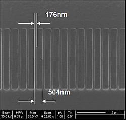 |
| Grating etched into LiNbO3 planar waveguides. The etched air gap width is 388 nm and depth is about 800nm |
Abstract:
Siyuan Yu, Professor in Photonics and Optical Communications
Department of Electrical & Electronic Engineering, University of Bristol
Photonic Structures Fabrication in LiNbO3 Crystals using the System100 ICP180
UK | Posted on June 14th, 2010The Photonics Group at the University of Bristol have used their OIPT System100 RIE100 ICP180 system to develop a high speed, high quality process for etching sub-micron features in Lithium Niobate (LiNbO3) and related materials. This work was motivated by the need to produce high aspect ratio, highly vertical features, such as photonic crystals, in LiNbO3.
LiNbO3 is a hard material to etch. Previously reported etch processes had limited dry etch rate of ~20 nm/min. Such slow etch rate was also typically associated with low selectivity over mask materials. Although the slow etch processes may be able to etch waveguides that does not require very vertical profiles, they require a long etch time. More importantly, they cannot be used to achieve photonic features with sizes approaching 100nm and requiring very smooth and vertical sidewall profiles to optimise their optical performance.
The Bristol group developed an optimised SF6-based chemistry on the RIE100/ICP180 system. The high density ICP plasma source enables etch rates of up to 200 nm/min, with vertical and smooth sidewalls. Ridge waveguides, gratings (Figure 1), and photonic crystals (Figure 2) have been successfully etched into LiNbO3 planar waveguide layers produced by proto exchange and by epitaxial growth on Lithium Tantalate (LiTaO3) substrates. Depths of up to 0.8 micron have been achieved with feature sizes of less than 200 nm.
The Bristol group have also been able to pattern the LiTaO3 substrate using such etching processes before the epitaxial growth of the LiNbO3 layer at Prof Pam Thomas' group in the Physics Department, Warwick University, who successfully produced buried photonic structures in these crystals.
####
For more information, please click here
Contacts:
Prof. Siyuan Yu.
Copyright © Oxford Instruments
If you have a comment, please Contact us.Issuers of news releases, not 7th Wave, Inc. or Nanotechnology Now, are solely responsible for the accuracy of the content.
Bookmark:


| Related News Press |
News and information
![]() Simulating magnetization in a Heisenberg quantum spin chain April 5th, 2024
Simulating magnetization in a Heisenberg quantum spin chain April 5th, 2024
![]() NRL charters Navy�s quantum inertial navigation path to reduce drift April 5th, 2024
NRL charters Navy�s quantum inertial navigation path to reduce drift April 5th, 2024
![]() Discovery points path to flash-like memory for storing qubits: Rice find could hasten development of nonvolatile quantum memory April 5th, 2024
Discovery points path to flash-like memory for storing qubits: Rice find could hasten development of nonvolatile quantum memory April 5th, 2024
Possible Futures
![]() Discovery points path to flash-like memory for storing qubits: Rice find could hasten development of nonvolatile quantum memory April 5th, 2024
Discovery points path to flash-like memory for storing qubits: Rice find could hasten development of nonvolatile quantum memory April 5th, 2024
![]() With VECSELs towards the quantum internet Fraunhofer: IAF achieves record output power with VECSEL for quantum frequency converters April 5th, 2024
With VECSELs towards the quantum internet Fraunhofer: IAF achieves record output power with VECSEL for quantum frequency converters April 5th, 2024
Academic/Education
![]() Rice University launches Rice Synthetic Biology Institute to improve lives January 12th, 2024
Rice University launches Rice Synthetic Biology Institute to improve lives January 12th, 2024
![]() Multi-institution, $4.6 million NSF grant to fund nanotechnology training September 9th, 2022
Multi-institution, $4.6 million NSF grant to fund nanotechnology training September 9th, 2022
Announcements
![]() NRL charters Navy�s quantum inertial navigation path to reduce drift April 5th, 2024
NRL charters Navy�s quantum inertial navigation path to reduce drift April 5th, 2024
![]() Discovery points path to flash-like memory for storing qubits: Rice find could hasten development of nonvolatile quantum memory April 5th, 2024
Discovery points path to flash-like memory for storing qubits: Rice find could hasten development of nonvolatile quantum memory April 5th, 2024
Photonics/Optics/Lasers
![]() With VECSELs towards the quantum internet Fraunhofer: IAF achieves record output power with VECSEL for quantum frequency converters April 5th, 2024
With VECSELs towards the quantum internet Fraunhofer: IAF achieves record output power with VECSEL for quantum frequency converters April 5th, 2024
![]() Nanoscale CL thermometry with lanthanide-doped heavy-metal oxide in TEM March 8th, 2024
Nanoscale CL thermometry with lanthanide-doped heavy-metal oxide in TEM March 8th, 2024
![]() Optically trapped quantum droplets of light can bind together to form macroscopic complexes March 8th, 2024
Optically trapped quantum droplets of light can bind together to form macroscopic complexes March 8th, 2024
![]() HKUST researchers develop new integration technique for efficient coupling of III-V and silicon February 16th, 2024
HKUST researchers develop new integration technique for efficient coupling of III-V and silicon February 16th, 2024
|
|
||
|
|
||
| The latest news from around the world, FREE | ||
|
|
||
|
|
||
| Premium Products | ||
|
|
||
|
Only the news you want to read!
Learn More |
||
|
|
||
|
Full-service, expert consulting
Learn More |
||
|
|
||