Home > Press > Applied physicists create building blocks for a new class of optical circuits
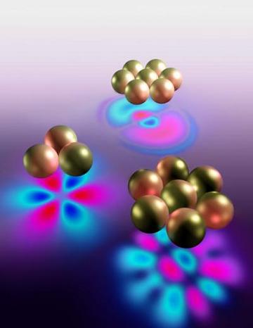 |
| Schematics of two types of optical circuits: the three particle trimer functions as a nanoscale magnet, while the seven particle heptamer exhibits almost no scattering for a narrow range of wavelengths due to interference. Credit: The laboratory of Federico Cappaso, Harvard School of Engineering and Applied Sciences |
Abstract:
Scalable devices inspired by nature exhibit customizable optical properties suitable for applications ranging from highly sensitive sensors and detectors to invisibility cloaks
Applied physicists create building blocks for a new class of optical circuits
Cambridge, MA | Posted on June 2nd, 2010Imagine creating novel devices with amazing and exotic optical properties not found in nature�by simply evaporating a droplet of particles on a surface.
By chemically building clusters of nanospheres from a liquid, a team of Harvard researchers, in collaboration with scientists at Rice University, the University of Texas at Austin, and the University of Houston, has developed just that.
The finding, published in the May 28 issue of Science, demonstrates simple scalable devices that exhibit customizable optical properties suitable for applications ranging from highly sensitive sensors and detectors to invisibility cloaks. Using particles consisting of concentric metallic and insulating shells, Jonathan Fan, a graduate student at the Harvard School of Engineering and Applied Sciences (SEAS), his lead co-author Federico Capasso, Robert L. Wallace Professor of Applied Physics and Vinton Hayes Senior Research Fellow in Electrical Engineering at SEAS, and Vinothan Manoharan, Associate professor of Chemical Engineering and Physics at SEAS and Harvard's Physics Department, devised a bottom-up, self-assembly approach to meet the design challenge.
"A longstanding challenge in optical engineering has been to find ways to make structures of size much smaller than the wavelength that exhibit desired and interesting properties," says Fan. "At visible frequencies, these structures must be nanoscale."
In contrast, most nanoscale devices are fabricated using top-down approaches, akin to how computer chips are manufactured. The smallest sizes that can be realized by such techniques are severely constrained by the intrinsic limits of the fabrication process, such as the wavelength of light used in the process. Moreover, such methods are restricted to planar geometries, are expensive, and require intense infrastructure such as cleanrooms.
"With our bottom-up approach, we mimic the way nature creates innovative structures, which exhibit extremely useful properties," explains Capasso. "Our nanoclusters behave as tiny optical circuits and could be the basis of new technology such as detectors of single molecules, efficient and biologically compatible probes in cancer therapeutics, and optical tweezers to manipulate and sort out nano-sized particles. Moreover, the fabrication process is much simpler and cheaper to carry out."
The researcher's self-assembly method requires nothing more than a bit of mixing and drying. To form the clusters, the particles are first coated with a polymer, and a droplet of them is then evaporated on a water-repellent surface. In the process of evaporation, the particles pack together into small clusters. Using polymer spacers to separate the nanoparticles, the researchers were able to controllably achieve a two nanometer gap between the particles�far better resolution than traditional top-down methods allow.
Two types of resulting optical circuits are of considerable interest. A trimer, comprising three equally-spaced particles, can support a magnetic response, an essential property of invisibility cloaks and materials that exhibit negative refractive index.
"In essence, the trimer acts as a nanoscale resonator that can support a circulating loop of current at visible and near-infrared frequencies," says Fan. "This structure functions as a nanoscale magnet at optical frequencies, something that natural materials cannot do."
Heptamers, or packed seven particle structures, exhibit almost no scattering for a narrow range of well-defined colors or wavelengths when illuminated with white light. These sharp dips, known as Fano resonances, arise from the interference of two modes of electron oscillations, a "bright" mode and a non-optically active "dark" mode, in the nanoparticle.
"Heptamers are very efficient at creating extremely intense electric fields localized in nanometer-size regions where molecules and nanoscale particles can be trapped, manipulated, and detected. Molecular sensing would rely on detecting shifts in the narrow spectra dips," says Capasso.
Ultimately, all of the self-assembled circuit designs can be readily tuned by varying the geometry, how the particles are separated, and the chemical environment. In short, the new method allows a "tool kit" for manipulating "artificial molecules" in such a way to create optical properties at will, a feature the researchers expect is broadly generalizable to a host of other characteristics.
Looking ahead, the researchers plan to work on achieving higher cluster yields and hope to assemble three-dimensional structures at the macroscale, a "holy grail" of materials science.
"We are excited by the potentially scalability of the method," says Manoharan. "Spheres are the easiest shapes to assemble as they can be readily packed together. While we only demonstrated here planar particle clusters, our method can be extended to three-dimensional structures, something that a top-down approach would have difficulty doing."
Fan, Capasso, and Manoharan's co-authors included Chihhui Wu and Gennady Shvets of University of Texas at Austin; Jiming Bao of the University of Houston; and Kui Bao, Rizia Bardhan, Naomi Halas, and Peter Norlander, all of Rice University.
The researchers acknowledge the support of National Science Foundation, the Air Force Office of Scientific Research; the U.S. Department of Defense; the Robert A. Welch Foundation; and the Center for Advanced Solar Photophysics, a U.S. Department of Energy Frontier Research Center. The work was carried out at the Center for Nanoscale Systems at Harvard, a member of the National Nanotechnology Infrastructure Network.
####
For more information, please click here
Contacts:
Michael Patrick Rutter
617-496-3815
Copyright © Harvard University
If you have a comment, please Contact us.Issuers of news releases, not 7th Wave, Inc. or Nanotechnology Now, are solely responsible for the accuracy of the content.
Bookmark:


| Related News Press |
News and information
![]() Simulating magnetization in a Heisenberg quantum spin chain April 5th, 2024
Simulating magnetization in a Heisenberg quantum spin chain April 5th, 2024
![]() NRL charters Navy�s quantum inertial navigation path to reduce drift April 5th, 2024
NRL charters Navy�s quantum inertial navigation path to reduce drift April 5th, 2024
![]() Discovery points path to flash-like memory for storing qubits: Rice find could hasten development of nonvolatile quantum memory April 5th, 2024
Discovery points path to flash-like memory for storing qubits: Rice find could hasten development of nonvolatile quantum memory April 5th, 2024
Govt.-Legislation/Regulation/Funding/Policy
![]() NRL charters Navy�s quantum inertial navigation path to reduce drift April 5th, 2024
NRL charters Navy�s quantum inertial navigation path to reduce drift April 5th, 2024
![]() Discovery points path to flash-like memory for storing qubits: Rice find could hasten development of nonvolatile quantum memory April 5th, 2024
Discovery points path to flash-like memory for storing qubits: Rice find could hasten development of nonvolatile quantum memory April 5th, 2024
![]() Chemical reactions can scramble quantum information as well as black holes April 5th, 2024
Chemical reactions can scramble quantum information as well as black holes April 5th, 2024
Possible Futures
![]() Discovery points path to flash-like memory for storing qubits: Rice find could hasten development of nonvolatile quantum memory April 5th, 2024
Discovery points path to flash-like memory for storing qubits: Rice find could hasten development of nonvolatile quantum memory April 5th, 2024
![]() With VECSELs towards the quantum internet Fraunhofer: IAF achieves record output power with VECSEL for quantum frequency converters April 5th, 2024
With VECSELs towards the quantum internet Fraunhofer: IAF achieves record output power with VECSEL for quantum frequency converters April 5th, 2024
Academic/Education
![]() Rice University launches Rice Synthetic Biology Institute to improve lives January 12th, 2024
Rice University launches Rice Synthetic Biology Institute to improve lives January 12th, 2024
![]() Multi-institution, $4.6 million NSF grant to fund nanotechnology training September 9th, 2022
Multi-institution, $4.6 million NSF grant to fund nanotechnology training September 9th, 2022
Self Assembly
![]() Liquid crystal templated chiral nanomaterials October 14th, 2022
Liquid crystal templated chiral nanomaterials October 14th, 2022
![]() Nanoclusters self-organize into centimeter-scale hierarchical assemblies April 22nd, 2022
Nanoclusters self-organize into centimeter-scale hierarchical assemblies April 22nd, 2022
![]() Atom by atom: building precise smaller nanoparticles with templates March 4th, 2022
Atom by atom: building precise smaller nanoparticles with templates March 4th, 2022
![]() Nanostructures get complex with electron equivalents: Nanoparticles of two different sizes break away from symmetrical designs January 14th, 2022
Nanostructures get complex with electron equivalents: Nanoparticles of two different sizes break away from symmetrical designs January 14th, 2022
Nanomedicine
![]() New micromaterial releases nanoparticles that selectively destroy cancer cells April 5th, 2024
New micromaterial releases nanoparticles that selectively destroy cancer cells April 5th, 2024
![]() Good as gold - improving infectious disease testing with gold nanoparticles April 5th, 2024
Good as gold - improving infectious disease testing with gold nanoparticles April 5th, 2024
![]() Researchers develop artificial building blocks of life March 8th, 2024
Researchers develop artificial building blocks of life March 8th, 2024
Sensors
Announcements
![]() NRL charters Navy�s quantum inertial navigation path to reduce drift April 5th, 2024
NRL charters Navy�s quantum inertial navigation path to reduce drift April 5th, 2024
![]() Discovery points path to flash-like memory for storing qubits: Rice find could hasten development of nonvolatile quantum memory April 5th, 2024
Discovery points path to flash-like memory for storing qubits: Rice find could hasten development of nonvolatile quantum memory April 5th, 2024
Tools
![]() Ferroelectrically modulate the Fermi level of graphene oxide to enhance SERS response November 3rd, 2023
Ferroelectrically modulate the Fermi level of graphene oxide to enhance SERS response November 3rd, 2023
![]() The USTC realizes In situ electron paramagnetic resonance spectroscopy using single nanodiamond sensors November 3rd, 2023
The USTC realizes In situ electron paramagnetic resonance spectroscopy using single nanodiamond sensors November 3rd, 2023
Photonics/Optics/Lasers
![]() With VECSELs towards the quantum internet Fraunhofer: IAF achieves record output power with VECSEL for quantum frequency converters April 5th, 2024
With VECSELs towards the quantum internet Fraunhofer: IAF achieves record output power with VECSEL for quantum frequency converters April 5th, 2024
![]() Nanoscale CL thermometry with lanthanide-doped heavy-metal oxide in TEM March 8th, 2024
Nanoscale CL thermometry with lanthanide-doped heavy-metal oxide in TEM March 8th, 2024
![]() Optically trapped quantum droplets of light can bind together to form macroscopic complexes March 8th, 2024
Optically trapped quantum droplets of light can bind together to form macroscopic complexes March 8th, 2024
![]() HKUST researchers develop new integration technique for efficient coupling of III-V and silicon February 16th, 2024
HKUST researchers develop new integration technique for efficient coupling of III-V and silicon February 16th, 2024
Research partnerships
![]() Discovery points path to flash-like memory for storing qubits: Rice find could hasten development of nonvolatile quantum memory April 5th, 2024
Discovery points path to flash-like memory for storing qubits: Rice find could hasten development of nonvolatile quantum memory April 5th, 2024
![]() Researchers� approach may protect quantum computers from attacks March 8th, 2024
Researchers� approach may protect quantum computers from attacks March 8th, 2024
![]() 'Sudden death' of quantum fluctuations defies current theories of superconductivity: Study challenges the conventional wisdom of superconducting quantum transitions January 12th, 2024
'Sudden death' of quantum fluctuations defies current theories of superconductivity: Study challenges the conventional wisdom of superconducting quantum transitions January 12th, 2024
|
|
||
|
|
||
| The latest news from around the world, FREE | ||
|
|
||
|
|
||
| Premium Products | ||
|
|
||
|
Only the news you want to read!
Learn More |
||
|
|
||
|
Full-service, expert consulting
Learn More |
||
|
|
||