Home > Press > Plasmonic Promises: First Observation of Plasmarons in Graphene
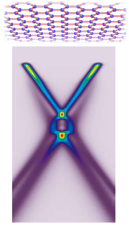 |
| A theoretical model of plasmaron interactions in graphene, sheets of carbon one atom thick. |
Abstract:
Scientists working at the Advanced Light Source (ALS) at the U.S. Department of Energy's Lawrence Berkeley National Laboratory have discovered striking new details about the electronic structure of graphene, crystalline sheets of carbon just one atom thick. An international team led by Aaron Bostwick and Eli Rotenberg of the ALS found that composite particles called plasmarons play a vital role in determining graphene's properties.
Plasmonic Promises: First Observation of Plasmarons in Graphene
Berkeley, CA | Posted on May 21st, 2010"The interesting properties of graphene are all collective phenomena," says Rotenberg, an ALS senior staff scientist responsible for the scientific program at ALS beamline 7, where the work was performed. "Graphene's true electronic structure can't be understood without understanding the many complex interactions of electrons with other particles."
The electric charge carriers in graphene are negative electrons and positive holes, which in turn are affected by plasmons�density oscillations that move like sound waves through the "liquid" of all the electrons in the material. A plasmaron is a composite particle, a charge carrier coupled with a plasmon.
"Although plasmarons were proposed theoretically in the late 1960s, and indirect evidence of them has been found, our work is the first observation of their distinct energy bands in graphene, or indeed in any material," Rotenberg says.
Understanding the relationships among these three kinds of particles�charge carriers, plasmons, and plasmarons�may hasten the day when graphene can be used for "plasmonics" to build ultrafast computers�perhaps even room-temperature quantum computers�plus a wide range of other tools and applications.
Strange graphene gets stranger
"Graphene has no band gap," says Bostwick, a research scientist on beamline 7.0.1 and lead author of the study. "On the usual band-gap diagram of neutral graphene, the filled valence band and the empty conduction band are shown as two cones, which meet at their tips at a point called the Dirac crossing."
Graphene is unique in that electrons near the Dirac crossing move as if they have no mass, traveling at a significant fraction of the speed of light. Plasmons couple directly to these elementary charges. Their frequencies may reach 100 trillion cycles per second (100 terahertz, 100 THz)�much higher than the frequency of conventional electronics in today's computers, which typically operate at about a few billion cycles per second (a few gigahertz, GHz).
Plasmons can also be excited by photons, particles of light, from external sources. Photonics is the field that includes the control and use of light for information processing; plasmons can be directed through channels measured on the nanoscale (billionths of a meter), much smaller than in conventional photonic devices.
And since the density of graphene's electric charge carriers can easily be influenced, it is straightforward to tune the electronic properties of graphene nanostructures. For these and other reasons, says Bostwick, "graphene is a promising candidate for much smaller, much faster devices�nanoscale plasmonic devices that merge electronics and photonics."
The usual picture of graphene's simple conical bands is not a complete description, however; instead it's an idealized picture of "bare" electrons. Not only do electrons (and holes) continually interact with each other and other entities, the traditional band-gap picture fails to predict the newly discovered plasmarons revealed by Bostwick and his collaborators.
The team reports their findings and discuss the implications in "Observations of plasmarons in quasi-free-standing doped graphene," by Aaron Bostwick, Florian Speck, Thomas Seyller, Karsten Horn, Marco Polini, Reza Asgari, Allan H. MacDonald, and Eli Rotenberg, in the 21 May 2010 issue of Science, available online to subscribers.
Graphene is most familiar as the individual layers that make up graphite, the pencil-lead form of carbon; what makes graphite soft and a good lubricant is that the single-atom layers readily slide over one another, their atoms strongly bonded in the plane but weakly bonded between planes. Since the 1980s, graphene sheets have been rolled-up into carbon nanotubes or closed buckyball spheroids. Theorists long doubted that single graphene sheets could exist unless stacked or closed in on themselves.
Then in 2004 single graphene sheets were isolated, and graphene has since been used in many experiments. Graphene sheets suspended in vacuum don't work for the kind of electronic studies that Bostwick and Rotenberg perform at ALS beamline 7.0.1. They use a technique known as angle-resolved photoemission spectroscopy (ARPES); for ARPES, the surface of the sample must be flat. Free-standing graphene is rarely flat; at best it resembles a crumpled bedsheet.
Using electrons to draw images of composite particles
"One of the best ways to grow a flat sheet of graphene is by heating a crystal of silicon carbide," Rotenberg says, "and it happens that our German colleagues Thomas Seyller from the University of Erlangen and Karsten Horn from the Fritz Haber Institute in Berlin are experts at working with silicon carbide. As the silicon recedes from the surface it leaves a single carbon layer."
Using flat graphene made this way, the researchers hoped to study graphene's intrinsic properties by ARPES. First a beam of soft x-rays from the ALS frees electrons from the graphene (photoemission). Then by measuring the direction (angle) and speed of the emitted electrons, the experiment recovers their energy and momentum; the spectrum of the cumulative emitted electrons is transmitted directly onto a two-dimensional detector.
The result is an image of the electronic bands created by the electrons themselves. In the case of graphene, the picture is x shaped, a cross-sectional cut through the two conical bands.
"Even in our initial experiments with graphene, we suspected that the ARPES distribution was not quite as simple as the two-cone, bare-electron model suggested," Rotenberg says. "At low resolution there appeared to be a kink in the bands at the Dirac crossing." Because there really is no such thing as a bare electron, the researchers wondered if this fuzziness was caused by charge carriers emitting plasmons.
"But theorists thought we should see even stronger effects," says Rotenberg, "and so we wondered if the substrate was influencing the physics. A single layer of carbon atoms resting on a silicon carbide substrate isn't the same as free-standing graphene."
The silicon-carbide substrate could in principle weaken the interactions between charges in the graphene (on most substrates the electronic properties of graphene are disturbed, and the plasmonic effects can't be observed). Therefore the team introduced hydrogen atoms that bonded to the underlying silicon carbide, isolating the graphene layer from the substrate and reducing its influence. Now the graphene film was flat enough to study with ARPES but sufficiently isolated to reveal its intrinsic interactions.
The images obtained by ARPES actually reflect the dynamics of the holes left behind after photoemission of the electrons. The lifetime and mass of excited holes are strongly subject to scattering from other excitations such as phonons (vibrations of the atoms in the crystal lattice), or by creating new electron-hole pairs.
"In the case of graphene, the electron can leave behind either an ordinary hole or a hole bound to a plasmon�a plasmaron," says Rotenberg.
Taken together, the interactions dramatically influenced the ARPES spectrum. When the researchers deposited potassium atoms atop the layer of carbon atoms to add extra electrons to the graphene, a detailed ARPES picture of the Dirac crossing region emerged. It revealed that the energy bands of graphene cross at three places, not one.
Ordinary holes have two conical bands that meet at a single point, just as in the bare-electron, non-interacting picture. But another pair of conical bands, the plasmaron bands, meets at a second, lower Dirac crossing. Between these crossings lies a ring where the hole and plasmaron bands cross.
"By their nature, plasmons couple strongly to photons, which promises new ways for manipulating light in nanostructures, giving rise to the field of plasmonics," Rotenberg says. "Now we know that plasmons couple strongly to the charge carriers in graphene, which suggests that graphene may have an important role to play in the merging fields of electronics, photonics, and plasmonics on the nanoscale."
This research was supported by the DOE Office of Science.
####
About Berkeley Lab
Berkeley Lab is a U.S. Department of Energy national laboratory located in Berkeley, California. It conducts unclassified scientific research for DOE�s Office of Science and is managed by the University of California. Visit our website at www.lbl.gov.
For more information, please click here
Contacts:
Paul Preuss
510-486-6249
Scientific contact:
Eli Rotenberg
510-486-5975
Copyright © Berkeley Lab
If you have a comment, please Contact us.Issuers of news releases, not 7th Wave, Inc. or Nanotechnology Now, are solely responsible for the accuracy of the content.
Bookmark:


| Related News Press |
News and information
![]() Simulating magnetization in a Heisenberg quantum spin chain April 5th, 2024
Simulating magnetization in a Heisenberg quantum spin chain April 5th, 2024
![]() NRL charters Navy�s quantum inertial navigation path to reduce drift April 5th, 2024
NRL charters Navy�s quantum inertial navigation path to reduce drift April 5th, 2024
![]() Discovery points path to flash-like memory for storing qubits: Rice find could hasten development of nonvolatile quantum memory April 5th, 2024
Discovery points path to flash-like memory for storing qubits: Rice find could hasten development of nonvolatile quantum memory April 5th, 2024
Govt.-Legislation/Regulation/Funding/Policy
![]() NRL charters Navy�s quantum inertial navigation path to reduce drift April 5th, 2024
NRL charters Navy�s quantum inertial navigation path to reduce drift April 5th, 2024
![]() Discovery points path to flash-like memory for storing qubits: Rice find could hasten development of nonvolatile quantum memory April 5th, 2024
Discovery points path to flash-like memory for storing qubits: Rice find could hasten development of nonvolatile quantum memory April 5th, 2024
![]() Chemical reactions can scramble quantum information as well as black holes April 5th, 2024
Chemical reactions can scramble quantum information as well as black holes April 5th, 2024
Possible Futures
![]() Discovery points path to flash-like memory for storing qubits: Rice find could hasten development of nonvolatile quantum memory April 5th, 2024
Discovery points path to flash-like memory for storing qubits: Rice find could hasten development of nonvolatile quantum memory April 5th, 2024
![]() With VECSELs towards the quantum internet Fraunhofer: IAF achieves record output power with VECSEL for quantum frequency converters April 5th, 2024
With VECSELs towards the quantum internet Fraunhofer: IAF achieves record output power with VECSEL for quantum frequency converters April 5th, 2024
Nanotubes/Buckyballs/Fullerenes/Nanorods/Nanostrings
![]() Tests find no free-standing nanotubes released from tire tread wear September 8th, 2023
Tests find no free-standing nanotubes released from tire tread wear September 8th, 2023
![]() Detection of bacteria and viruses with fluorescent nanotubes July 21st, 2023
Detection of bacteria and viruses with fluorescent nanotubes July 21st, 2023
Nanoelectronics
![]() Interdisciplinary: Rice team tackles the future of semiconductors Multiferroics could be the key to ultralow-energy computing October 6th, 2023
Interdisciplinary: Rice team tackles the future of semiconductors Multiferroics could be the key to ultralow-energy computing October 6th, 2023
![]() Key element for a scalable quantum computer: Physicists from Forschungszentrum J�lich and RWTH Aachen University demonstrate electron transport on a quantum chip September 23rd, 2022
Key element for a scalable quantum computer: Physicists from Forschungszentrum J�lich and RWTH Aachen University demonstrate electron transport on a quantum chip September 23rd, 2022
![]() Reduced power consumption in semiconductor devices September 23rd, 2022
Reduced power consumption in semiconductor devices September 23rd, 2022
![]() Atomic level deposition to extend Moore�s law and beyond July 15th, 2022
Atomic level deposition to extend Moore�s law and beyond July 15th, 2022
Discoveries
![]() Chemical reactions can scramble quantum information as well as black holes April 5th, 2024
Chemical reactions can scramble quantum information as well as black holes April 5th, 2024
![]() New micromaterial releases nanoparticles that selectively destroy cancer cells April 5th, 2024
New micromaterial releases nanoparticles that selectively destroy cancer cells April 5th, 2024
![]() Utilizing palladium for addressing contact issues of buried oxide thin film transistors April 5th, 2024
Utilizing palladium for addressing contact issues of buried oxide thin film transistors April 5th, 2024
Announcements
![]() NRL charters Navy�s quantum inertial navigation path to reduce drift April 5th, 2024
NRL charters Navy�s quantum inertial navigation path to reduce drift April 5th, 2024
![]() Discovery points path to flash-like memory for storing qubits: Rice find could hasten development of nonvolatile quantum memory April 5th, 2024
Discovery points path to flash-like memory for storing qubits: Rice find could hasten development of nonvolatile quantum memory April 5th, 2024
Photonics/Optics/Lasers
![]() With VECSELs towards the quantum internet Fraunhofer: IAF achieves record output power with VECSEL for quantum frequency converters April 5th, 2024
With VECSELs towards the quantum internet Fraunhofer: IAF achieves record output power with VECSEL for quantum frequency converters April 5th, 2024
![]() Nanoscale CL thermometry with lanthanide-doped heavy-metal oxide in TEM March 8th, 2024
Nanoscale CL thermometry with lanthanide-doped heavy-metal oxide in TEM March 8th, 2024
![]() Optically trapped quantum droplets of light can bind together to form macroscopic complexes March 8th, 2024
Optically trapped quantum droplets of light can bind together to form macroscopic complexes March 8th, 2024
![]() HKUST researchers develop new integration technique for efficient coupling of III-V and silicon February 16th, 2024
HKUST researchers develop new integration technique for efficient coupling of III-V and silicon February 16th, 2024
|
|
||
|
|
||
| The latest news from around the world, FREE | ||
|
|
||
|
|
||
| Premium Products | ||
|
|
||
|
Only the news you want to read!
Learn More |
||
|
|
||
|
Full-service, expert consulting
Learn More |
||
|
|
||