Home > Press > How Things Work: Atomic force microscopy
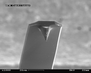 |
| Electron microscopy allows us to see the cantilever of an atomic force microscope. This cantilever applies force to a surface, producing an accurate image of the surface. Courtesy of Wikimedia Commons. |
Abstract:
Atomic force microscopy (AFM), a popular tool for imaging, measuring, and manipulating matter at the nanoscale, was invented in 1986 and was commercialized in 1989. This type of microscopy gathers information by feeling the surface with mechanical probes. AFM is a type of scanning probe microscopy (SPM) in which the image of a surface is obtained by moving a probe over a sample and recording the interactions between the probe and the surface of the sample.
By Kush Mangal
How Things Work: Atomic force microscopy
Pittsburgh, PA | Posted on April 26th, 2010AFM is used for a variety of biological applications, including imaging molecules, cells, tissues, and biomaterials. At Carnegie Mellon, AFM is being used to study peptides and lipoproteins. AFM, popularly used in nanotechnology research, has been used to image the surface of the ivy plant to understand how it climbs structures, as stated in an article on www.photonics.com.
According to www.veeco.com, AFM is on the cutting edge of science since it provides true three-dimensional surface images. AFM is used to image and manipulate atoms and structures on many different surfaces. Samples viewed by AFM do not need any special treatments. The technology provides higher resolution images than other methods such as the scanning electron microscope. It is also favorable since it has the ability to operate in liquids and work with sample sizes ranging from a few nanometers up to several micrometers.
An AFM consists of several important components: a scanner (which is mounted above the tip or below the sample), a detector, and feedback controls. A cantilever moves over the surface of a sample in a scan. The cantilever is usually composed of silicon or silicon nitride, and has a sharp tip on one side that interacts with surface of a sample. The type of tip used depends on the sample it will interact with. The scanner is made from a tube of piezoelectric elements, which are materials that change shape when a certain amount of voltage is applied to them. According to the optical level method for the detector, a laser beam is shot at the tip of the cantilever and is reflected onto a position-sensitive photo-detector.
According to the book Atomic Force Microscopy: Biomedical Methods and Applications, AFM can operate in several modes: force-distance, contact, and tapping mode. In the force-distance mode, the tip will start above the surface and is brought down. When the tip is close to the surface, it sticks to it and then retracts back to the starting point. In the contact mode, the tip contacts the surface, and the tip will deflect up and down based on the sample's topography. The force feedback from the tip ensures that there is contact with the surface. Contact mode provides information about physical properties such as elasticity, adhesion, hardness, and friction. In tapping mode, the cantilever is oscillated and brought into contact with the surface. The contact with the sample is intermittent over a very short time. The changing amplitude of the oscillation provides information about the surface. Tapping mode is a better choice with soft samples since it is less damaging, while contact mode is most useful for hard surfaces.
The tip used in AFM is one of the important factors influencing the resolution obtained. The sharper the tip used, the greater the resolution. The tip can be affected by different parameters to alter the image. These are compression, interaction forces, and irregular curvatures. Compression affects studies with DNA, irregular curvatures cause broadening in the image, and interaction forces cause an increase in image contrast.
AFM is a great tool for visualization on the atomic scale. The images it provides of both conductive and nonconductive materials are valuable to researchers. AFM allows for a different way to visualize molecules in three dimensions.
####
About Carnegie Mellon University
Carnegie Mellon University is a global research university with more than 11,000 students, 75,000 active alumni, and 4,000 faculty and staff. Recognized for its world-class arts and technology programs, collaboration across disciplines and innovative leadership in education, Carnegie Mellon is consistently a top-ranked university.
For more information, please click here
Copyright © Carnegie Mellon
If you have a comment, please Contact us.Issuers of news releases, not 7th Wave, Inc. or Nanotechnology Now, are solely responsible for the accuracy of the content.
Bookmark:


| Related News Press |
News and information
![]() Simulating magnetization in a Heisenberg quantum spin chain April 5th, 2024
Simulating magnetization in a Heisenberg quantum spin chain April 5th, 2024
![]() NRL charters Navy�s quantum inertial navigation path to reduce drift April 5th, 2024
NRL charters Navy�s quantum inertial navigation path to reduce drift April 5th, 2024
![]() Discovery points path to flash-like memory for storing qubits: Rice find could hasten development of nonvolatile quantum memory April 5th, 2024
Discovery points path to flash-like memory for storing qubits: Rice find could hasten development of nonvolatile quantum memory April 5th, 2024
Academic/Education
![]() Rice University launches Rice Synthetic Biology Institute to improve lives January 12th, 2024
Rice University launches Rice Synthetic Biology Institute to improve lives January 12th, 2024
![]() Multi-institution, $4.6 million NSF grant to fund nanotechnology training September 9th, 2022
Multi-institution, $4.6 million NSF grant to fund nanotechnology training September 9th, 2022
Tools
![]() Ferroelectrically modulate the Fermi level of graphene oxide to enhance SERS response November 3rd, 2023
Ferroelectrically modulate the Fermi level of graphene oxide to enhance SERS response November 3rd, 2023
![]() The USTC realizes In situ electron paramagnetic resonance spectroscopy using single nanodiamond sensors November 3rd, 2023
The USTC realizes In situ electron paramagnetic resonance spectroscopy using single nanodiamond sensors November 3rd, 2023
|
|
||
|
|
||
| The latest news from around the world, FREE | ||
|
|
||
|
|
||
| Premium Products | ||
|
|
||
|
Only the news you want to read!
Learn More |
||
|
|
||
|
Full-service, expert consulting
Learn More |
||
|
|
||