Home > Press > Shining Light on Graphene-Metal Interactions
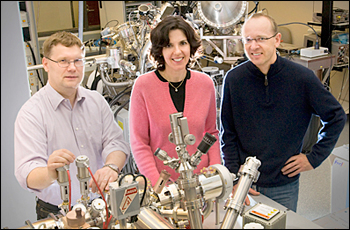 |
| From left, Jurek Sadowski, Eli Sutter, and Peter Sutter |
Abstract:
By controlling the layered growth of graphene - a relatively "new" form of carbon that's just a single atom thick - researchers at Brookhaven National Laboratory have uncovered intriguing details about the material's superior electrical and optical properties. Their findings could help position graphene as the next-generation material for future computers, digital displays, and electronic sensors.
By Kendra Snyder
Shining Light on Graphene-Metal Interactions
Upton, NY | Posted on April 2nd, 2010"Graphene is a material that really has the potential to replace silicon in the electronics industry," said Peter Sutter, a materials scientist in Brookhaven's Center for Functional Nanomaterials. "It's thin, transparent, strong, and highly conductive - all extremely appealing characteristics for everything from computer chips to touch screens and solar cells."
One of the biggest challenges facing researchers is figuring out how to produce graphene in large quantities. The simplest method is peeling off single sheets of graphene from graphite, a material consisting of many graphene layers, with pieces of tape. But this method yields only small, jagged flakes that aren't useful for most applications.
At Brookhaven, Sutter's group grows graphene on a metal substrate, a technique that can produce single-layer sheets over very large areas, thousands of times larger than the pieces made with the "Scotch tape" method. First, a single crystal of ruthenium is heated up to temperatures higher than 1000 degrees Celsius while being exposed to a carbon-rich gas. At high temperatures, carbon atoms are able to squeeze into spaces within the metal crystal, similar to water being taken in by a sponge. As the crystal is slowly cooled, these carbon atoms are expelled to the surface of the metal, where they form individual layers of graphene. The number of layers formed can be controlled by the amount of carbon atoms initially absorbed into the ruthenium crystal.
"One of the unique aspects of this method is that we can control the thickness of the material, growing graphene layer by layer," Sutter said. "This has allowed us to see how the structure and electronic properties of the material change as single atomic carbon layers are added to the substrate one at a time."
Because the research group wanted to determine how the metal substrate affects the properties of graphene, it was important to monitor the layered material's characteristics as it was grown � a capability provided by a special microscope at the National Synchrotron Light Source.
"First, we were able to watch how the material grew, and then, without moving it from the system, we were able to switch on the photon beam and determine its electronic structure," Stutter said. "It's extremely valuable to do everything in the same environment."
To obtain measurements for the material with different numbers of graphene sheets, the group used micro-angle-resolved photoelectron spectroscopy, a technique that allows researchers to study the electronic structure of very small regions of interest.
Their findings, published in the July 8, 2009 edition of Nano Letters, were surprising.
"We found that if a single graphene sheet is grown on a metal like ruthenium, the metal binds very strongly to the carbon atoms and disrupts the characteristic properties normally found in isolated graphene," Sutter said. "But those properties re-emerge in subsequent layers grown on the substrate."
In other words, the first graphene layer grown on ruthenium satiates the metal substrate, allowing the rest of the layers to reclaim their normal properties.
"As a result of this growth process, a two-layer stack acts like an isolated monolayer of graphene and a three-layer stack acts like an isolated bilayer," Sutter said.
The findings of the group, which also includes Brookhaven researchers Mark Hybertsen, Jurek Sadowski, and Eli Sutter, lays groundwork for future graphene production for advanced technologies, and helps researchers understand how metals � for example in device contacts � change the properties of graphene.
This work was funded by the U.S. Department of Energy Office of Basic Energy Sciences within the Office of Science.
####
About Brookhaven National Laboratory
One of ten national laboratories overseen and primarily funded by the Office of Science of the U.S. Department of Energy (DOE), Brookhaven National Laboratory conducts research in the physical, biomedical, and environmental sciences, as well as in energy technologies and national security. Brookhaven Lab also builds and operates major scientific facilities available to university, industry and government researchers. Brookhaven is operated and managed for DOE's Office of Science by Brookhaven Science Associates, a limited-liability company founded by Stony Brook University, the largest academic user of Laboratory facilities, and Battelle, a nonprofit, applied science and technology organization.
For more information, please click here
Copyright © Brookhaven National Laboratory
If you have a comment, please Contact us.Issuers of news releases, not 7th Wave, Inc. or Nanotechnology Now, are solely responsible for the accuracy of the content.
Bookmark:


| Related News Press |
News and information
![]() Simulating magnetization in a Heisenberg quantum spin chain April 5th, 2024
Simulating magnetization in a Heisenberg quantum spin chain April 5th, 2024
![]() NRL charters Navy�s quantum inertial navigation path to reduce drift April 5th, 2024
NRL charters Navy�s quantum inertial navigation path to reduce drift April 5th, 2024
![]() Discovery points path to flash-like memory for storing qubits: Rice find could hasten development of nonvolatile quantum memory April 5th, 2024
Discovery points path to flash-like memory for storing qubits: Rice find could hasten development of nonvolatile quantum memory April 5th, 2024
![]() Good as gold - improving infectious disease testing with gold nanoparticles April 5th, 2024
Good as gold - improving infectious disease testing with gold nanoparticles April 5th, 2024
Display technology/LEDs/SS Lighting/OLEDs
![]() Utilizing palladium for addressing contact issues of buried oxide thin film transistors April 5th, 2024
Utilizing palladium for addressing contact issues of buried oxide thin film transistors April 5th, 2024
![]() Light guide plate based on perovskite nanocomposites November 3rd, 2023
Light guide plate based on perovskite nanocomposites November 3rd, 2023
![]() Simple ballpoint pen can write custom LEDs August 11th, 2023
Simple ballpoint pen can write custom LEDs August 11th, 2023
Govt.-Legislation/Regulation/Funding/Policy
![]() NRL charters Navy�s quantum inertial navigation path to reduce drift April 5th, 2024
NRL charters Navy�s quantum inertial navigation path to reduce drift April 5th, 2024
![]() Discovery points path to flash-like memory for storing qubits: Rice find could hasten development of nonvolatile quantum memory April 5th, 2024
Discovery points path to flash-like memory for storing qubits: Rice find could hasten development of nonvolatile quantum memory April 5th, 2024
![]() Chemical reactions can scramble quantum information as well as black holes April 5th, 2024
Chemical reactions can scramble quantum information as well as black holes April 5th, 2024
Possible Futures
![]() Discovery points path to flash-like memory for storing qubits: Rice find could hasten development of nonvolatile quantum memory April 5th, 2024
Discovery points path to flash-like memory for storing qubits: Rice find could hasten development of nonvolatile quantum memory April 5th, 2024
![]() With VECSELs towards the quantum internet Fraunhofer: IAF achieves record output power with VECSEL for quantum frequency converters April 5th, 2024
With VECSELs towards the quantum internet Fraunhofer: IAF achieves record output power with VECSEL for quantum frequency converters April 5th, 2024
Chip Technology
![]() Discovery points path to flash-like memory for storing qubits: Rice find could hasten development of nonvolatile quantum memory April 5th, 2024
Discovery points path to flash-like memory for storing qubits: Rice find could hasten development of nonvolatile quantum memory April 5th, 2024
![]() Utilizing palladium for addressing contact issues of buried oxide thin film transistors April 5th, 2024
Utilizing palladium for addressing contact issues of buried oxide thin film transistors April 5th, 2024
![]() HKUST researchers develop new integration technique for efficient coupling of III-V and silicon February 16th, 2024
HKUST researchers develop new integration technique for efficient coupling of III-V and silicon February 16th, 2024
Nanotubes/Buckyballs/Fullerenes/Nanorods/Nanostrings
![]() Tests find no free-standing nanotubes released from tire tread wear September 8th, 2023
Tests find no free-standing nanotubes released from tire tread wear September 8th, 2023
![]() Detection of bacteria and viruses with fluorescent nanotubes July 21st, 2023
Detection of bacteria and viruses with fluorescent nanotubes July 21st, 2023
Sensors
Nanoelectronics
![]() Interdisciplinary: Rice team tackles the future of semiconductors Multiferroics could be the key to ultralow-energy computing October 6th, 2023
Interdisciplinary: Rice team tackles the future of semiconductors Multiferroics could be the key to ultralow-energy computing October 6th, 2023
![]() Key element for a scalable quantum computer: Physicists from Forschungszentrum J�lich and RWTH Aachen University demonstrate electron transport on a quantum chip September 23rd, 2022
Key element for a scalable quantum computer: Physicists from Forschungszentrum J�lich and RWTH Aachen University demonstrate electron transport on a quantum chip September 23rd, 2022
![]() Reduced power consumption in semiconductor devices September 23rd, 2022
Reduced power consumption in semiconductor devices September 23rd, 2022
![]() Atomic level deposition to extend Moore�s law and beyond July 15th, 2022
Atomic level deposition to extend Moore�s law and beyond July 15th, 2022
Materials/Metamaterials/Magnetoresistance
![]() Nanoscale CL thermometry with lanthanide-doped heavy-metal oxide in TEM March 8th, 2024
Nanoscale CL thermometry with lanthanide-doped heavy-metal oxide in TEM March 8th, 2024
![]() Focused ion beam technology: A single tool for a wide range of applications January 12th, 2024
Focused ion beam technology: A single tool for a wide range of applications January 12th, 2024
Announcements
![]() NRL charters Navy�s quantum inertial navigation path to reduce drift April 5th, 2024
NRL charters Navy�s quantum inertial navigation path to reduce drift April 5th, 2024
![]() Discovery points path to flash-like memory for storing qubits: Rice find could hasten development of nonvolatile quantum memory April 5th, 2024
Discovery points path to flash-like memory for storing qubits: Rice find could hasten development of nonvolatile quantum memory April 5th, 2024
Solar/Photovoltaic
![]() Development of zinc oxide nanopagoda array photoelectrode: photoelectrochemical water-splitting hydrogen production January 12th, 2024
Development of zinc oxide nanopagoda array photoelectrode: photoelectrochemical water-splitting hydrogen production January 12th, 2024
![]() Shedding light on unique conduction mechanisms in a new type of perovskite oxide November 17th, 2023
Shedding light on unique conduction mechanisms in a new type of perovskite oxide November 17th, 2023
![]() Inverted perovskite solar cell breaks 25% efficiency record: Researchers improve cell efficiency using a combination of molecules to address different November 17th, 2023
Inverted perovskite solar cell breaks 25% efficiency record: Researchers improve cell efficiency using a combination of molecules to address different November 17th, 2023
![]() Charged �molecular beasts� the basis for new compounds: Researchers at Leipzig University use �aggressive� fragments of molecular ions for chemical synthesis November 3rd, 2023
Charged �molecular beasts� the basis for new compounds: Researchers at Leipzig University use �aggressive� fragments of molecular ions for chemical synthesis November 3rd, 2023
|
|
||
|
|
||
| The latest news from around the world, FREE | ||
|
|
||
|
|
||
| Premium Products | ||
|
|
||
|
Only the news you want to read!
Learn More |
||
|
|
||
|
Full-service, expert consulting
Learn More |
||
|
|
||