Home > Press > Helium-Ion Microscopy Fires the Imagination of Researchers in U.S. and Japan
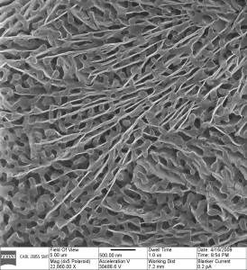 |
| One of EMSL's priorities is to research mineral to mineral and mineral to microbial filaments. This ORION image (figure 1) shows mineral filaments interpenetrating porous silicon. Even though the uncoated, insulating sample suffered from charging when imaged by a scanning electron microscope (SEM), the helium-ion microscope produced superior resolution images with no charging problems. (Photo: Business Wire) |
Abstract:
The Pacific Northwest National Laboratory (PNNL) and The National Institute of Advanced Industrial Science and Technology (AIST) have recently ordered ORION® PLUS Helium-Ion Microscopes from Carl Zeiss.
Helium-Ion Microscopy Fires the Imagination of Researchers in U.S. and Japan
Peabody, MA | Posted on March 31st, 2010The Pacific Northwest National Laboratory (PNNL), located in Richland, Washington, is bringing an ORION® PLUS instrument into the U.S. Department of Energy's Environmental Molecular Sciences Laboratory as a resource. And, in Tsukuba, Japan, the National Institute of Advanced Industrial Science and Technology (AIST) has selected an ORION PLUS for their new Nanodevice Innovation Research Center. These installations provide further evidence of a growing reliance on helium-ion microscopy for the most demanding research in materials, life science and semiconductor applications.
PNNL has become the first US national lab to acquire a ZEISS ORION PLUS helium-ion microscope. One of the Department of Energy's (DOE's) ten national laboratories, managed by DOE's Office of Science, PNNL offers an open, collaborative environment for scientific discovery to researchers around the world. "We are very excited to be adding a helium-ion microscope to our arsenal of leading-edge scientific instruments," said Shuttha Shutthanadan, scientist at the Environmental Molecular Sciences Laboratory (EMSL), a national scientific user facility located at PNNL. "Basically, helium-ion microscopy improves our vision at the nanoscale, allowing us to see things we could never see before. Having access to an instrument that provides world-record spatial resolution imaging, plus high image contrast and large depth of field will enable our users to accelerate their innovations."
Weilin Jiang, EMSL scientist, adds, "Perhaps one of the greatest advantages of helium-ion microscopy is the ability to clearly image uncoated insulating materials." This circumvents the time consuming, resolution diminishing practice of coating a sample to deal with its charging. The tool is scheduled for delivery at the end of March of this year.
At the prestigious AIST in Tsukuba, Japan, formal acceptance of their new ORION PLUS microscope was completed on February eighth of this year. The AIST system is outfitted with all of the available options, including the recently developed Spectra Detector. A newly designed Gas Injection System will be added shortly. "Installation and acceptance were completed rapidly and without any major issues, including a dramatic trip by crane to a fourth floor balcony of the AIST building," reports David Voci, Carl Zeiss SMT's director of business development for the ORION product. AIST will use the tool in support of their research into next generation semiconductor technology, as well as for clean energy applications.
Research topics identified include Low K dielectrics, EUV photomask metrology, nano-imprint lithography, carbon nanotube and graphene device research, as well as applications in support of solar and fuel cell research. The instrument is situated in a user facility that eventually will be available to all AIST researchers for a broad range of uses from semiconductor to life science applications. "The AIST system was the first ORION PLUS microscope delivered that was designed and built to achieve the 0.35nm probe size specification. The EMSL ORION PLUS instrument is the second tool of this generation, and we are confident that our production and field service team will accomplish this installation equally well as with the AIST system," comments Voci.
####
About Carl Zeiss
The Carl Zeiss Group is a leading group of companies operating worldwide in the optical and opto-electronic industries that generates revenues totaling around EUR 2.1 billion (2008/09). Carl Zeiss offers innovative solutions for the future-oriented markets of Medical and Research Solutions, Industrial Solutions and Lifestyle Products. The Carl Zeiss Group has approximately 13,000 employees worldwide, including more than 8,000 in Germany. The Carl Zeiss business groups hold leading positions in their markets. Carl Zeiss AG, Oberkochen, is fully owned by the Carl Zeiss Stiftung (Carl Zeiss Foundation).
Carl Zeiss SMT
Carl Zeiss SMT AG comprises the Semiconductor Technology Group of the Carl Zeiss Group. Carl Zeiss SMT is one of the leading manufacturers of lithography optics and light, electron and ion-optical inspection, analysis and measuring systems. The company offers a broad spectrum of application and service solutions for the fields of semiconductor technology, nanotechnology, materials research and life sciences. Carl Zeiss SMT AG is headquartered in Oberkochen, Germany. Other sites are located in Germany, the UK, France, the USA, Israel and Singapore. The company has a global workforce of over 2,500 people and generated revenues of just under EUR 400 million in fiscal year 2008/09. Carl Zeiss SMT AG is fully owned by Carl Zeiss AG, Oberkochen. Further information is available at www.smt.zeiss.com
Pacific Northwest National Laboratory
The Pacific Northwest National Laboratory is a Department of Energy Office of Science national laboratory where interdisciplinary teams advance science and technology and deliver solutions to America's most intractable problems in energy, national security and the environment. PNNL employs 4,700 staff, has a $1.1 billion annual budget, and has been managed by Ohio-based Battelle since the lab's inception in 1965. Follow PNNL on Facebook , Linked In and Twitter
Environmental Molecular Sciences Laboratory
EMSL, the Environmental Molecular Sciences Laboratory, is a national scientific user facility sponsored by the Department of Energy's Office of Science, Biological and Environmental Research program that is located at Pacific Northwest National Laboratory. EMSL offers an open, collaborative environment for scientific discovery to researchers around the world. EMSL's technical experts and suite of custom and advanced instruments are unmatched. Its integrated computational and experimental capabilities enable researchers to realize fundamental scientific insights and create new technologies. Follow EMSL on Facebook.
National Institute of Advanced Industrial Science and Technology
The National Institute of Advanced Industrial Science and Technology, led by President Dr. Nomakuchi, is a public institution that is funded largely by the Japanese government. The present AIST is a rather new research organization established in 2001, however, AIST and its predecessor organizations have been contributing to society through continuous advancement in technologies and support of Japanese industries since 1876.
Headquarters of AIST are located in Tsukuba and Tokyo. AIST has over 50 autonomous research units in various innovative research fields, and the units are located at 9 research bases and several sites (smaller than research bases) of AIST all over Japan. About 2500 research scientists (about 2000 with tenure) and well over 3000 visiting scientists, post doctoral fellows and students are working at AIST. About 700 permanent administrative personnel and many temporary staff support the research work of AIST.
For more information, please click here
Contacts:
Carl Zeiss SMT AG, Germany
Markus Wiederspahn
+49 73 64 20 21 94
Public Relations
or
Carl Zeiss SMT, Inc., NA
Bill Monigle
941-497-1622
Public Relations, North America
Copyright © Business Wire
If you have a comment, please Contact us.Issuers of news releases, not 7th Wave, Inc. or Nanotechnology Now, are solely responsible for the accuracy of the content.
Bookmark:


| Related News Press |
News and information
![]() Simulating magnetization in a Heisenberg quantum spin chain April 5th, 2024
Simulating magnetization in a Heisenberg quantum spin chain April 5th, 2024
![]() NRL charters Navy’s quantum inertial navigation path to reduce drift April 5th, 2024
NRL charters Navy’s quantum inertial navigation path to reduce drift April 5th, 2024
![]() Discovery points path to flash-like memory for storing qubits: Rice find could hasten development of nonvolatile quantum memory April 5th, 2024
Discovery points path to flash-like memory for storing qubits: Rice find could hasten development of nonvolatile quantum memory April 5th, 2024
Chip Technology
![]() Discovery points path to flash-like memory for storing qubits: Rice find could hasten development of nonvolatile quantum memory April 5th, 2024
Discovery points path to flash-like memory for storing qubits: Rice find could hasten development of nonvolatile quantum memory April 5th, 2024
![]() Utilizing palladium for addressing contact issues of buried oxide thin film transistors April 5th, 2024
Utilizing palladium for addressing contact issues of buried oxide thin film transistors April 5th, 2024
![]() HKUST researchers develop new integration technique for efficient coupling of III-V and silicon February 16th, 2024
HKUST researchers develop new integration technique for efficient coupling of III-V and silicon February 16th, 2024
Nanotubes/Buckyballs/Fullerenes/Nanorods/Nanostrings
![]() Tests find no free-standing nanotubes released from tire tread wear September 8th, 2023
Tests find no free-standing nanotubes released from tire tread wear September 8th, 2023
![]() Detection of bacteria and viruses with fluorescent nanotubes July 21st, 2023
Detection of bacteria and viruses with fluorescent nanotubes July 21st, 2023
Nanomedicine
![]() New micromaterial releases nanoparticles that selectively destroy cancer cells April 5th, 2024
New micromaterial releases nanoparticles that selectively destroy cancer cells April 5th, 2024
![]() Good as gold - improving infectious disease testing with gold nanoparticles April 5th, 2024
Good as gold - improving infectious disease testing with gold nanoparticles April 5th, 2024
![]() Researchers develop artificial building blocks of life March 8th, 2024
Researchers develop artificial building blocks of life March 8th, 2024
Nanoelectronics
![]() Interdisciplinary: Rice team tackles the future of semiconductors Multiferroics could be the key to ultralow-energy computing October 6th, 2023
Interdisciplinary: Rice team tackles the future of semiconductors Multiferroics could be the key to ultralow-energy computing October 6th, 2023
![]() Key element for a scalable quantum computer: Physicists from Forschungszentrum Jülich and RWTH Aachen University demonstrate electron transport on a quantum chip September 23rd, 2022
Key element for a scalable quantum computer: Physicists from Forschungszentrum Jülich and RWTH Aachen University demonstrate electron transport on a quantum chip September 23rd, 2022
![]() Reduced power consumption in semiconductor devices September 23rd, 2022
Reduced power consumption in semiconductor devices September 23rd, 2022
![]() Atomic level deposition to extend Moore’s law and beyond July 15th, 2022
Atomic level deposition to extend Moore’s law and beyond July 15th, 2022
Announcements
![]() NRL charters Navy’s quantum inertial navigation path to reduce drift April 5th, 2024
NRL charters Navy’s quantum inertial navigation path to reduce drift April 5th, 2024
![]() Discovery points path to flash-like memory for storing qubits: Rice find could hasten development of nonvolatile quantum memory April 5th, 2024
Discovery points path to flash-like memory for storing qubits: Rice find could hasten development of nonvolatile quantum memory April 5th, 2024
Tools
![]() Ferroelectrically modulate the Fermi level of graphene oxide to enhance SERS response November 3rd, 2023
Ferroelectrically modulate the Fermi level of graphene oxide to enhance SERS response November 3rd, 2023
![]() The USTC realizes In situ electron paramagnetic resonance spectroscopy using single nanodiamond sensors November 3rd, 2023
The USTC realizes In situ electron paramagnetic resonance spectroscopy using single nanodiamond sensors November 3rd, 2023
Nanobiotechnology
![]() New micromaterial releases nanoparticles that selectively destroy cancer cells April 5th, 2024
New micromaterial releases nanoparticles that selectively destroy cancer cells April 5th, 2024
![]() Good as gold - improving infectious disease testing with gold nanoparticles April 5th, 2024
Good as gold - improving infectious disease testing with gold nanoparticles April 5th, 2024
![]() Researchers develop artificial building blocks of life March 8th, 2024
Researchers develop artificial building blocks of life March 8th, 2024
Alliances/Trade associations/Partnerships/Distributorships
![]() Chicago Quantum Exchange welcomes six new partners highlighting quantum technology solutions, from Chicago and beyond September 23rd, 2022
Chicago Quantum Exchange welcomes six new partners highlighting quantum technology solutions, from Chicago and beyond September 23rd, 2022
![]() University of Illinois Chicago joins Brookhaven Lab's Quantum Center June 10th, 2022
University of Illinois Chicago joins Brookhaven Lab's Quantum Center June 10th, 2022
|
|
||
|
|
||
| The latest news from around the world, FREE | ||
|
|
||
|
|
||
| Premium Products | ||
|
|
||
|
Only the news you want to read!
Learn More |
||
|
|
||
|
Full-service, expert consulting
Learn More |
||
|
|
||