Home > Press > New Path To Solar Energy Via Solid-State Photovoltaics
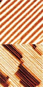 |
| These nanoscale images of bismuth ferrite thin films show ordered arrays of 71 degree domain walls (top) and 109 degree doman walls (bottom). By changing the polarization direction of the bismuth ferrite, these domain walls give rise to the photovoltaic effect. (Image from Seidel, et. al.) |
Abstract:
A newly discovered path for the conversion of sunlight to electricity could brighten the future for photovoltaic technology. Researchers with Lawrence Berkeley National Laboratory (Berkeley Lab) have found a new mechanism by which the photovoltaic effect can take place in semiconductor thin-films. This new route to energy production overcomes the bandgap voltage limitation that continues to plague conventional solid-state solar cells.
New Path To Solar Energy Via Solid-State Photovoltaics
Berkeley, CA | Posted on March 31st, 2010Working with bismuth ferrite, a ceramic made from bismuth, iron and oxygen that is multiferroic - meaning it simultaneously displays both ferroelectric and ferromagnetic properties - the researchers discovered that the photovoltaic effect can spontaneously arise at the nanoscale as a result of the ceramic's rhombohedrally distorted crystal structure. Furthermore, they demonstrated that the application of an electric field makes it possible to manipulate this crystal structure and thereby control photovoltaic properties.
"We're excited to find functionality that has not been seen before at the nanoscale in a multiferroic material," said Jan Seidel, a physicist who holds joint appointments with Berkeley Lab's Materials Sciences Division and the UC Berkeley Physics Department. "We're now working on transferring this concept to higher efficiency energy-research related devices."
Seidel is one of the lead authors of a paper in the journal Nature Nanotechnology that describes this work titled, "Above-bandgap voltages from ferroelectric photovoltaic devices." Co-authoring this paper with Seidel were Seung-Yeul Yang, Steven Byrnes, Padraic Shafer,Chan-Ho Yang, Marta Rossell, Pu Yu, Ying-Hao Chu, James Scott, Joel Ager, Lane Martin and Ramamoorthy Ramesh.
At the heart of conventional solid-state solar cells is a p-n junction, the interface between a semiconductor layer with an abundance of positively-charged "holes," and a layer with an abundance of negatively charged electrons. When photons from the sun are absorbed, their energy creates electron-hole pairs that can be separated within a "depletion zone," a microscopic region at the p-n junction measuring only a couple of micrometers across, then collected as electricity. For this process to take place, however, the photons have to penetrate the material to the depletion zone and their energy has to precisely match the energy of the semiconductor's electronic bandgap - the gap between its valence and conduction energy bands where no electron states can exist.
"The maximum voltage conventional solid-state photovoltaic devices can produce is equal to the energy of their electronic bandgap," Seidel says. "Even for so called tandem-cells, in which several semiconductor p-n junctions are stacked, photovoltages are still limited because of the finite penetration depth of light into the material."
Working through Berkeley Lab's Helios Solar Energy Research Center, Seidel and his collaborators discovered that by applying white light to bismuth ferrite, a material that is both ferroelectric and antiferromagnetic, they could generate photovoltages within submicroscopic areas between one and two nanometers across. These photovoltages were significantly higher than bismuth ferrite's electronic bandgap.
"The bandgap energy of the bismuth ferrite is equivalent to 2.7 volts. From our measurements we know that with our mechanism we can get approximately 16 volts over a distance of 200 microns. Furthermore, this voltage is in principle linear scalable, which means that larger distances should lead to higher voltages."
Behind this new mechanism for photovoltage generation are domain walls - two-dimensional sheets that run through a multiferroic and serve as transition zones, separating regions of different ferromagnetic or ferroelectric properties. In their study, Seidel and his collaborators found that these domain walls can serve the same electron-hole separation purpose as depletion zones only with distinct advantages.
"The much smaller scale of these domain walls enables a great many of them to be stacked laterally (sideways) and still be reached by light," Seidel says. "This in turn makes it possible to increase the photovoltage values well above the electronic bandgap of the material."
The photovoltaic effect arises because at the domain walls the polarization direction of the bismuth ferrite changes, which leads to steps in the electrostatic potential. Through annealing treatments of the substrate upon which bismuth ferrite is grown, the material's rhombohedral crystals can be induced to form domain walls that change the direction of electric field polarization by either 71, 109 or 180 degrees. Seidel and his collaborators measured the photovoltages created by the 71 and 109 degree domain walls.
"The 71 degree domain walls showed unidirectional in-plane polarization alignment and produced an aligned series of potential voltage steps," Seidel says. "Although the potential step at the 109 degree domain was higher than the 71 degree domain, it showed two variants of the in-plane polarization which ran in opposite directions."
Seidel and his colleagues were also able to use a 200 volt electric pulse to either reverse the polarity of the photovoltaic effect or turn it off altogether. Such controllability of the photovoltaic effect has never been reported in conventional photovoltaic systems, and it paves the way for new applications in nano-optics and nano-electronics.
"While we have not yet demonstrated these possible new applications and devices, we believe that our research will stimulate concepts and thoughts that are based on this new direction for the photovoltaic effect," Seidel says.
Additional Information
For more information on the Helios Solar Energy Research Center, visit the Website at www.lbl.gov/LBL-Programs/helios-serc/index.html
####
About Berkeley Lab
Berkeley Lab is a U.S. Department of Energy national laboratory located in Berkeley, California. It conducts unclassified scientific research and is managed by the University of California. Visit our website at www.lbl.gov.
For more information, please click here
Contacts:
Lynn Yarris
(510) 486-5375
Copyright © Berkeley Lab
If you have a comment, please Contact us.Issuers of news releases, not 7th Wave, Inc. or Nanotechnology Now, are solely responsible for the accuracy of the content.
Bookmark:


| Related News Press |
News and information
![]() Simulating magnetization in a Heisenberg quantum spin chain April 5th, 2024
Simulating magnetization in a Heisenberg quantum spin chain April 5th, 2024
![]() NRL charters Navy�s quantum inertial navigation path to reduce drift April 5th, 2024
NRL charters Navy�s quantum inertial navigation path to reduce drift April 5th, 2024
![]() Discovery points path to flash-like memory for storing qubits: Rice find could hasten development of nonvolatile quantum memory April 5th, 2024
Discovery points path to flash-like memory for storing qubits: Rice find could hasten development of nonvolatile quantum memory April 5th, 2024
![]() Good as gold - improving infectious disease testing with gold nanoparticles April 5th, 2024
Good as gold - improving infectious disease testing with gold nanoparticles April 5th, 2024
Thin films
![]() Utilizing palladium for addressing contact issues of buried oxide thin film transistors April 5th, 2024
Utilizing palladium for addressing contact issues of buried oxide thin film transistors April 5th, 2024
![]() Understanding the mechanism of non-uniform formation of diamond film on tools: Paving the way to a dry process with less environmental impact March 24th, 2023
Understanding the mechanism of non-uniform formation of diamond film on tools: Paving the way to a dry process with less environmental impact March 24th, 2023
![]() New study introduces the best graphite films: The work by Distinguished Professor Feng Ding at UNIST has been published in the October 2022 issue of Nature Nanotechnology November 4th, 2022
New study introduces the best graphite films: The work by Distinguished Professor Feng Ding at UNIST has been published in the October 2022 issue of Nature Nanotechnology November 4th, 2022
Possible Futures
![]() Discovery points path to flash-like memory for storing qubits: Rice find could hasten development of nonvolatile quantum memory April 5th, 2024
Discovery points path to flash-like memory for storing qubits: Rice find could hasten development of nonvolatile quantum memory April 5th, 2024
![]() With VECSELs towards the quantum internet Fraunhofer: IAF achieves record output power with VECSEL for quantum frequency converters April 5th, 2024
With VECSELs towards the quantum internet Fraunhofer: IAF achieves record output power with VECSEL for quantum frequency converters April 5th, 2024
Nanoelectronics
![]() Interdisciplinary: Rice team tackles the future of semiconductors Multiferroics could be the key to ultralow-energy computing October 6th, 2023
Interdisciplinary: Rice team tackles the future of semiconductors Multiferroics could be the key to ultralow-energy computing October 6th, 2023
![]() Key element for a scalable quantum computer: Physicists from Forschungszentrum J�lich and RWTH Aachen University demonstrate electron transport on a quantum chip September 23rd, 2022
Key element for a scalable quantum computer: Physicists from Forschungszentrum J�lich and RWTH Aachen University demonstrate electron transport on a quantum chip September 23rd, 2022
![]() Reduced power consumption in semiconductor devices September 23rd, 2022
Reduced power consumption in semiconductor devices September 23rd, 2022
![]() Atomic level deposition to extend Moore�s law and beyond July 15th, 2022
Atomic level deposition to extend Moore�s law and beyond July 15th, 2022
Discoveries
![]() Chemical reactions can scramble quantum information as well as black holes April 5th, 2024
Chemical reactions can scramble quantum information as well as black holes April 5th, 2024
![]() New micromaterial releases nanoparticles that selectively destroy cancer cells April 5th, 2024
New micromaterial releases nanoparticles that selectively destroy cancer cells April 5th, 2024
![]() Utilizing palladium for addressing contact issues of buried oxide thin film transistors April 5th, 2024
Utilizing palladium for addressing contact issues of buried oxide thin film transistors April 5th, 2024
Announcements
![]() NRL charters Navy�s quantum inertial navigation path to reduce drift April 5th, 2024
NRL charters Navy�s quantum inertial navigation path to reduce drift April 5th, 2024
![]() Discovery points path to flash-like memory for storing qubits: Rice find could hasten development of nonvolatile quantum memory April 5th, 2024
Discovery points path to flash-like memory for storing qubits: Rice find could hasten development of nonvolatile quantum memory April 5th, 2024
Energy
![]() Development of zinc oxide nanopagoda array photoelectrode: photoelectrochemical water-splitting hydrogen production January 12th, 2024
Development of zinc oxide nanopagoda array photoelectrode: photoelectrochemical water-splitting hydrogen production January 12th, 2024
![]() Shedding light on unique conduction mechanisms in a new type of perovskite oxide November 17th, 2023
Shedding light on unique conduction mechanisms in a new type of perovskite oxide November 17th, 2023
![]() Inverted perovskite solar cell breaks 25% efficiency record: Researchers improve cell efficiency using a combination of molecules to address different November 17th, 2023
Inverted perovskite solar cell breaks 25% efficiency record: Researchers improve cell efficiency using a combination of molecules to address different November 17th, 2023
![]() The efficient perovskite cells with a structured anti-reflective layer � another step towards commercialization on a wider scale October 6th, 2023
The efficient perovskite cells with a structured anti-reflective layer � another step towards commercialization on a wider scale October 6th, 2023
Photonics/Optics/Lasers
![]() With VECSELs towards the quantum internet Fraunhofer: IAF achieves record output power with VECSEL for quantum frequency converters April 5th, 2024
With VECSELs towards the quantum internet Fraunhofer: IAF achieves record output power with VECSEL for quantum frequency converters April 5th, 2024
![]() Nanoscale CL thermometry with lanthanide-doped heavy-metal oxide in TEM March 8th, 2024
Nanoscale CL thermometry with lanthanide-doped heavy-metal oxide in TEM March 8th, 2024
![]() Optically trapped quantum droplets of light can bind together to form macroscopic complexes March 8th, 2024
Optically trapped quantum droplets of light can bind together to form macroscopic complexes March 8th, 2024
![]() HKUST researchers develop new integration technique for efficient coupling of III-V and silicon February 16th, 2024
HKUST researchers develop new integration technique for efficient coupling of III-V and silicon February 16th, 2024
Solar/Photovoltaic
![]() Development of zinc oxide nanopagoda array photoelectrode: photoelectrochemical water-splitting hydrogen production January 12th, 2024
Development of zinc oxide nanopagoda array photoelectrode: photoelectrochemical water-splitting hydrogen production January 12th, 2024
![]() Shedding light on unique conduction mechanisms in a new type of perovskite oxide November 17th, 2023
Shedding light on unique conduction mechanisms in a new type of perovskite oxide November 17th, 2023
![]() Inverted perovskite solar cell breaks 25% efficiency record: Researchers improve cell efficiency using a combination of molecules to address different November 17th, 2023
Inverted perovskite solar cell breaks 25% efficiency record: Researchers improve cell efficiency using a combination of molecules to address different November 17th, 2023
![]() Charged �molecular beasts� the basis for new compounds: Researchers at Leipzig University use �aggressive� fragments of molecular ions for chemical synthesis November 3rd, 2023
Charged �molecular beasts� the basis for new compounds: Researchers at Leipzig University use �aggressive� fragments of molecular ions for chemical synthesis November 3rd, 2023
|
|
||
|
|
||
| The latest news from around the world, FREE | ||
|
|
||
|
|
||
| Premium Products | ||
|
|
||
|
Only the news you want to read!
Learn More |
||
|
|
||
|
Full-service, expert consulting
Learn More |
||
|
|
||