 |
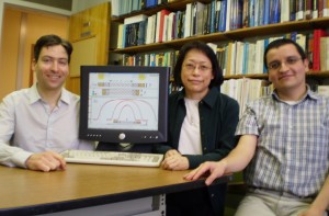
| Georgia Tech researchers Markus Kindermann, Mei-Yin Chou and Salvador Barraza-Lopez pose with a graphic from their study of metal contacts on graphene. Georgia Tech Photo |
Abstract:
New Study Quantifies the Electron Transport Effects of Placing Metal Contacts onto Graphene
By John Toon
Making Contact
Atlanta, GA | Posted on March 15th, 2010Using large-scale supercomputer calculations, researchers have analyzed how the placement of metallic contacts on graphene changes the electron transport properties of the material as a factor of junction length, width and orientation. The work is believed to be the first quantitative study of electron transport through metal-graphene junctions to examine earlier models in significant detail.
Information on the ways in which attaching metal contacts affects electron transport in graphene will be important to scientists studying the material - and to designers who may one day fabricate electronic devices from the carbon-lattice material.
"Graphene devices will have to communicate with the external world, and that means we will have to fabricate contacts to transport current and data," said Mei-Yin Chou, a professor and department chair in the School of Physics at the Georgia Institute of Technology. "When they put metal contacts onto graphene to measure transport properties, researchers and device designers need to know that they may not be measuring the instrinsic properties of pristine graphene. Coupling between the contacts and the material must be taken into account."
Information on the effects of metal contacts on graphene was reported in the journal Physical Review Letters on February 19th. The research was supported by the U.S. Department of Energy, and involved interactions with researchers at the National Science Foundation (NSF)-supported Materials Research Science and Engineering Center (MRSEC) at Georgia Tech.
Using large-scale, first-principles calculations done at two different NSF-supported supercomputer centers, the Georgia Tech research team - which included postdoctoral fellows Salvador Barraza-Lopez and Mihajlo Vanevic, and assistant professor Markus Kindermann - conducted detailed atomic-level calculations of aluminum contacts grown on graphene.
The calculations studied two contacts up to 14 nanometers apart, with graphene suspended between them. In their calculations, the researchers allowed the aluminum to grow as it would in the real world, then studied how electron transfer was induced in the area surrounding the contacts.
"People have been able to come up with phenomenological models that they use to find out what the effects are with metallic contacts," Chou explained. "Our calculations went a few steps farther because we built contacts atom-by-atom. We built atomistically-resolved contacts, and by doing that, we solved this problem at the atomic level and tried to do everything consistent with quantum mechanics."
Because metals typically have excess electrons, physically attaching the contacts to graphene causes a charge transfer from the metal. Charge begins to be transferred as soon as the contracts are constructed, but ultimately the two materials reach equilibrium, Chou said.
The study showed that charge transfer at the leads and into the freestanding section of the material creates an electron-hole asymmetry in the conductance. For leads that are sufficiently long, the effect creates two conductance minima at the energies of the Dirac points for the suspended and clamped regions of the graphene, according to Barraza-Lopez.
"These results could be important to the design of future graphene devices," he said. "Edge effects and the impact of nanoribbon width have been studied in significant detail, but the effects of charge transfer at the contacts may potentially be just as important."
The researchers modeled aluminum, but believe their results will apply to other metals such as copper and gold that do not form chemical bonds with graphene. However, other metals such as chromium and titanium do chemically alter the material, so the effects they have on electron transport may be different.
Beyond the new information provided by the calculations, the research further proposes quantitative models that can be used under certain circumstances to describe the impact of the contacts.
"Earlier models had been based on physical insights, but nobody really knew how faithfully they described the material," Kindermann said. "This is the first calculation to show that these earlier models apply under certain circumstances for the systems that we studied."
Data from the study may one day help device designers engineer graphene circuits by helping them understand the effects they are seeing.
"When we modify graphene, we need to understand what changes occur as a result of adding materials," added Chou. "This is really fundamental research to understand these effects and to have a numerical prediction for what is going on. We are helping to understand the basic physics of graphene."
This research was supported by Department of Energy grant DE-FG02-97ER45632. Comments and conclusions in this article are those of the researchers and do not necessarily reflect the views of the Department of Energy.
####
About Georgia Institute of Technology
The Georgia Institute of Technology is one of the nation's top research universities, distinguished by its commitment to improving the human condition through advanced science and technology.
Georgia Tech's campus occupies 400 acres in the heart of the city of Atlanta, where 20,000 undergraduate and graduate students receive a focused, technologically based education.
For more information, please click here
Contacts:
John Toon
404-894-6986
Abby Vogel
404-385-3364
Copyright © Georgia Institute of Technology
If you have a comment, please Contact us.Issuers of news releases, not 7th Wave, Inc. or Nanotechnology Now, are solely responsible for the accuracy of the content.
Bookmark:


| Related News Press |
News and information
![]() Simulating magnetization in a Heisenberg quantum spin chain April 5th, 2024
Simulating magnetization in a Heisenberg quantum spin chain April 5th, 2024
![]() NRL charters Navy�s quantum inertial navigation path to reduce drift April 5th, 2024
NRL charters Navy�s quantum inertial navigation path to reduce drift April 5th, 2024
![]() Discovery points path to flash-like memory for storing qubits: Rice find could hasten development of nonvolatile quantum memory April 5th, 2024
Discovery points path to flash-like memory for storing qubits: Rice find could hasten development of nonvolatile quantum memory April 5th, 2024
Preparing for Nano
![]() Disruptive by Design: Nano Now February 1st, 2019
Disruptive by Design: Nano Now February 1st, 2019
![]() How nanoscience will improve our health and lives in the coming years: Targeted medicine deliveries and increased energy efficiency are just two of many ways October 26th, 2016
How nanoscience will improve our health and lives in the coming years: Targeted medicine deliveries and increased energy efficiency are just two of many ways October 26th, 2016
![]() Searching for a nanotech self-organizing principle May 1st, 2016
Searching for a nanotech self-organizing principle May 1st, 2016
Govt.-Legislation/Regulation/Funding/Policy
![]() NRL charters Navy�s quantum inertial navigation path to reduce drift April 5th, 2024
NRL charters Navy�s quantum inertial navigation path to reduce drift April 5th, 2024
![]() Discovery points path to flash-like memory for storing qubits: Rice find could hasten development of nonvolatile quantum memory April 5th, 2024
Discovery points path to flash-like memory for storing qubits: Rice find could hasten development of nonvolatile quantum memory April 5th, 2024
![]() Chemical reactions can scramble quantum information as well as black holes April 5th, 2024
Chemical reactions can scramble quantum information as well as black holes April 5th, 2024
Academic/Education
![]() Rice University launches Rice Synthetic Biology Institute to improve lives January 12th, 2024
Rice University launches Rice Synthetic Biology Institute to improve lives January 12th, 2024
![]() Multi-institution, $4.6 million NSF grant to fund nanotechnology training September 9th, 2022
Multi-institution, $4.6 million NSF grant to fund nanotechnology training September 9th, 2022
Chip Technology
![]() Discovery points path to flash-like memory for storing qubits: Rice find could hasten development of nonvolatile quantum memory April 5th, 2024
Discovery points path to flash-like memory for storing qubits: Rice find could hasten development of nonvolatile quantum memory April 5th, 2024
![]() Utilizing palladium for addressing contact issues of buried oxide thin film transistors April 5th, 2024
Utilizing palladium for addressing contact issues of buried oxide thin film transistors April 5th, 2024
![]() HKUST researchers develop new integration technique for efficient coupling of III-V and silicon February 16th, 2024
HKUST researchers develop new integration technique for efficient coupling of III-V and silicon February 16th, 2024
Nanoelectronics
![]() Interdisciplinary: Rice team tackles the future of semiconductors Multiferroics could be the key to ultralow-energy computing October 6th, 2023
Interdisciplinary: Rice team tackles the future of semiconductors Multiferroics could be the key to ultralow-energy computing October 6th, 2023
![]() Key element for a scalable quantum computer: Physicists from Forschungszentrum J�lich and RWTH Aachen University demonstrate electron transport on a quantum chip September 23rd, 2022
Key element for a scalable quantum computer: Physicists from Forschungszentrum J�lich and RWTH Aachen University demonstrate electron transport on a quantum chip September 23rd, 2022
![]() Reduced power consumption in semiconductor devices September 23rd, 2022
Reduced power consumption in semiconductor devices September 23rd, 2022
![]() Atomic level deposition to extend Moore�s law and beyond July 15th, 2022
Atomic level deposition to extend Moore�s law and beyond July 15th, 2022
Announcements
![]() NRL charters Navy�s quantum inertial navigation path to reduce drift April 5th, 2024
NRL charters Navy�s quantum inertial navigation path to reduce drift April 5th, 2024
![]() Discovery points path to flash-like memory for storing qubits: Rice find could hasten development of nonvolatile quantum memory April 5th, 2024
Discovery points path to flash-like memory for storing qubits: Rice find could hasten development of nonvolatile quantum memory April 5th, 2024
Quantum nanoscience
![]() Simulating magnetization in a Heisenberg quantum spin chain April 5th, 2024
Simulating magnetization in a Heisenberg quantum spin chain April 5th, 2024
![]() Optically trapped quantum droplets of light can bind together to form macroscopic complexes March 8th, 2024
Optically trapped quantum droplets of light can bind together to form macroscopic complexes March 8th, 2024
![]() Bridging light and electrons January 12th, 2024
Bridging light and electrons January 12th, 2024
![]() 'Sudden death' of quantum fluctuations defies current theories of superconductivity: Study challenges the conventional wisdom of superconducting quantum transitions January 12th, 2024
'Sudden death' of quantum fluctuations defies current theories of superconductivity: Study challenges the conventional wisdom of superconducting quantum transitions January 12th, 2024
|
|
||
|
|
||
| The latest news from around the world, FREE | ||
|
|
||
|
|
||
| Premium Products | ||
|
|
||
|
Only the news you want to read!
Learn More |
||
|
|
||
|
Full-service, expert consulting
Learn More |
||
|
|
||