Home > Press > Trapping Sunlight with Silicon Nanowires
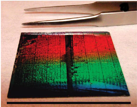 |
| This photovoltaic cell is comprised of 36 individual arrays of silicon nanowires featuring radial p-n junctions. The color dispersion demonstrates the excellent periodicity over the entire substrate. Photo by Peidong Yang. |
Abstract:
Solar cells made from silicon are projected to be a prominent factor in future renewable green energy equations, but so far the promise has far exceeded the reality. While there are now silicon photovoltaics that can convert sunlight into electricity at impressive 20 percent efficiencies, the cost of this solar power is prohibitive for large-scale use. Researchers with the Lawrence Berkeley National Laboratory (Berkeley Lab), however, are developing a new approach that could substantially reduce these costs. The key to their success is a better way of trapping sunlight.
Trapping Sunlight with Silicon Nanowires
Berkeley, CA | Posted on March 6th, 2010"Through the fabrication of thin films from ordered arrays of vertical silicon nanowires we've been able to increase the light-trapping in our solar cells by a factor of 73," says chemist Peidong Yang, who led this research. "Since the fabrication technique behind this extraordinary light-trapping enhancement is a relatively simple and scalable aqueous chemistry process, we believe our approach represents an economically viable path toward high-efficiency, low-cost thin-film solar cells."
Yang holds joint appointments with Berkeley Lab's Materials Sciences Division, and the University of California Berkeley's Chemistry Department. He is a leading authority on semiconductor nanowires - one-dimensional strips of materials whose width measures only one-thousandth that of a human hair but whose length may stretch several microns.
"Typical solar cells are made from very expensive ultrapure single crystal silicon wafers that require about 100 micrometers of thickness to absorb most of the solar light, whereas our radial geometry enables us to effectively trap light with nanowire arrays fabricated from silicon films that are only about eight micrometers thick," he says. "Furthermore, our approach should in principle allow us to use metallurgical grade or "dirty" silicon rather than the ultrapure silicon crystals now required, which should cut costs even further."
Yang has described this research in a paper published in the journal NANO Letters, which he co-authored with Erik Garnett, a chemist who was then a member of Yang's research group. The paper is titled "Light Trapping in Silicon Nanowire Solar Cells."
Generating Electricity from Sunlight
At the heart of all solar cells are two separate layers of material, one with an abundance of electrons that functions as a negative pole, and one with an abundance of electron holes (positively-charged energy spaces) that functions as a positive pole. When photons from the sun are absorbed, their energy is used to create electron-hole pairs, which are then separated at the interface between the two layers and collected as electricity.
Because of its superior photo-electronic properties, silicon remains the photovoltaic semiconductor of choice but rising demand has inflated the price of the raw material. Furthermore, because of the high-level of crystal purification required, even the fabrication of the simplest silicon-based solar cell is a complex, energy-intensive and costly process.
Yang and his group are able to reduce both the quantity and the quality requirements for silicon by using vertical arrays of nanostructured radial p-n junctions rather than conventional planar p-n junctions. In a radial p-n junction, a layer of n-type silicon forms a shell around a p-type silicon nanowire core. As a result, photo-excited electrons and holes travel much shorter distances to electrodes, eliminating a charge-carrier bottleneck that often arises in a typical silicon solar cell. The radial geometry array also, as photocurrent and optical transmission measurements by Yang and Garrett revealed, greatly improves light trapping.
"Since each individual nanowire in the array has a p-n junction, each acts as an individual solar cell," Yang says. "By adjusting the length of the nanowires in our arrays, we can increase their light-trapping path length."
While the conversion efficiency of these solar nanowires was only about five to six percent, Yang says this efficiency was achieved with little effort put into surface passivation, antireflection, and other efficiency-increasing modifications.
"With further improvements, most importantly in surface passivation, we think it is possible to push the efficiency to above 10 percent," Yang says.
Combining a 10 percent or better conversion efficiency with the greatly reduced quantities of starting silicon material and the ability to use metallurgical grade silicon, should make the use of silicon nanowires an attractive candidate for large-scale development.
As an added plus Yang says, "Our technique can be used in existing solar panel manufacturing processes."
This research was funded by the National Science Foundation's Center of Integrated Nanomechanical Systems.
Additional Information
For more about the research of Peidong Yang and his group, visit the Website at www.cchem.berkeley.edu/pdygrp/main.html
For more about the Center of Integrated Nanomechanical Systems (COINS) visit the Website at mint.physics.berkeley.edu/coins/
####
About Berkeley Lab
Berkeley Lab is a U.S. Department of Energy national laboratory located in Berkeley, California. It conducts unclassified scientific research for DOE�s Office of Science and is managed by the University of California. Visit our website at www.lbl.gov.
For more information, please click here
Contacts:
Lynn Yarris
(510) 486-5375
Copyright © Berkeley Lab
If you have a comment, please Contact us.Issuers of news releases, not 7th Wave, Inc. or Nanotechnology Now, are solely responsible for the accuracy of the content.
Bookmark:


| Related News Press |
News and information
![]() Simulating magnetization in a Heisenberg quantum spin chain April 5th, 2024
Simulating magnetization in a Heisenberg quantum spin chain April 5th, 2024
![]() NRL charters Navy�s quantum inertial navigation path to reduce drift April 5th, 2024
NRL charters Navy�s quantum inertial navigation path to reduce drift April 5th, 2024
![]() Discovery points path to flash-like memory for storing qubits: Rice find could hasten development of nonvolatile quantum memory April 5th, 2024
Discovery points path to flash-like memory for storing qubits: Rice find could hasten development of nonvolatile quantum memory April 5th, 2024
![]() Good as gold - improving infectious disease testing with gold nanoparticles April 5th, 2024
Good as gold - improving infectious disease testing with gold nanoparticles April 5th, 2024
Thin films
![]() Utilizing palladium for addressing contact issues of buried oxide thin film transistors April 5th, 2024
Utilizing palladium for addressing contact issues of buried oxide thin film transistors April 5th, 2024
![]() Understanding the mechanism of non-uniform formation of diamond film on tools: Paving the way to a dry process with less environmental impact March 24th, 2023
Understanding the mechanism of non-uniform formation of diamond film on tools: Paving the way to a dry process with less environmental impact March 24th, 2023
![]() New study introduces the best graphite films: The work by Distinguished Professor Feng Ding at UNIST has been published in the October 2022 issue of Nature Nanotechnology November 4th, 2022
New study introduces the best graphite films: The work by Distinguished Professor Feng Ding at UNIST has been published in the October 2022 issue of Nature Nanotechnology November 4th, 2022
Govt.-Legislation/Regulation/Funding/Policy
![]() NRL charters Navy�s quantum inertial navigation path to reduce drift April 5th, 2024
NRL charters Navy�s quantum inertial navigation path to reduce drift April 5th, 2024
![]() Discovery points path to flash-like memory for storing qubits: Rice find could hasten development of nonvolatile quantum memory April 5th, 2024
Discovery points path to flash-like memory for storing qubits: Rice find could hasten development of nonvolatile quantum memory April 5th, 2024
![]() Chemical reactions can scramble quantum information as well as black holes April 5th, 2024
Chemical reactions can scramble quantum information as well as black holes April 5th, 2024
Possible Futures
![]() Discovery points path to flash-like memory for storing qubits: Rice find could hasten development of nonvolatile quantum memory April 5th, 2024
Discovery points path to flash-like memory for storing qubits: Rice find could hasten development of nonvolatile quantum memory April 5th, 2024
![]() With VECSELs towards the quantum internet Fraunhofer: IAF achieves record output power with VECSEL for quantum frequency converters April 5th, 2024
With VECSELs towards the quantum internet Fraunhofer: IAF achieves record output power with VECSEL for quantum frequency converters April 5th, 2024
Academic/Education
![]() Rice University launches Rice Synthetic Biology Institute to improve lives January 12th, 2024
Rice University launches Rice Synthetic Biology Institute to improve lives January 12th, 2024
![]() Multi-institution, $4.6 million NSF grant to fund nanotechnology training September 9th, 2022
Multi-institution, $4.6 million NSF grant to fund nanotechnology training September 9th, 2022
Discoveries
![]() Chemical reactions can scramble quantum information as well as black holes April 5th, 2024
Chemical reactions can scramble quantum information as well as black holes April 5th, 2024
![]() New micromaterial releases nanoparticles that selectively destroy cancer cells April 5th, 2024
New micromaterial releases nanoparticles that selectively destroy cancer cells April 5th, 2024
![]() Utilizing palladium for addressing contact issues of buried oxide thin film transistors April 5th, 2024
Utilizing palladium for addressing contact issues of buried oxide thin film transistors April 5th, 2024
Announcements
![]() NRL charters Navy�s quantum inertial navigation path to reduce drift April 5th, 2024
NRL charters Navy�s quantum inertial navigation path to reduce drift April 5th, 2024
![]() Discovery points path to flash-like memory for storing qubits: Rice find could hasten development of nonvolatile quantum memory April 5th, 2024
Discovery points path to flash-like memory for storing qubits: Rice find could hasten development of nonvolatile quantum memory April 5th, 2024
Energy
![]() Development of zinc oxide nanopagoda array photoelectrode: photoelectrochemical water-splitting hydrogen production January 12th, 2024
Development of zinc oxide nanopagoda array photoelectrode: photoelectrochemical water-splitting hydrogen production January 12th, 2024
![]() Shedding light on unique conduction mechanisms in a new type of perovskite oxide November 17th, 2023
Shedding light on unique conduction mechanisms in a new type of perovskite oxide November 17th, 2023
![]() Inverted perovskite solar cell breaks 25% efficiency record: Researchers improve cell efficiency using a combination of molecules to address different November 17th, 2023
Inverted perovskite solar cell breaks 25% efficiency record: Researchers improve cell efficiency using a combination of molecules to address different November 17th, 2023
![]() The efficient perovskite cells with a structured anti-reflective layer � another step towards commercialization on a wider scale October 6th, 2023
The efficient perovskite cells with a structured anti-reflective layer � another step towards commercialization on a wider scale October 6th, 2023
Solar/Photovoltaic
![]() Development of zinc oxide nanopagoda array photoelectrode: photoelectrochemical water-splitting hydrogen production January 12th, 2024
Development of zinc oxide nanopagoda array photoelectrode: photoelectrochemical water-splitting hydrogen production January 12th, 2024
![]() Shedding light on unique conduction mechanisms in a new type of perovskite oxide November 17th, 2023
Shedding light on unique conduction mechanisms in a new type of perovskite oxide November 17th, 2023
![]() Inverted perovskite solar cell breaks 25% efficiency record: Researchers improve cell efficiency using a combination of molecules to address different November 17th, 2023
Inverted perovskite solar cell breaks 25% efficiency record: Researchers improve cell efficiency using a combination of molecules to address different November 17th, 2023
![]() Charged �molecular beasts� the basis for new compounds: Researchers at Leipzig University use �aggressive� fragments of molecular ions for chemical synthesis November 3rd, 2023
Charged �molecular beasts� the basis for new compounds: Researchers at Leipzig University use �aggressive� fragments of molecular ions for chemical synthesis November 3rd, 2023
|
|
||
|
|
||
| The latest news from around the world, FREE | ||
|
|
||
|
|
||
| Premium Products | ||
|
|
||
|
Only the news you want to read!
Learn More |
||
|
|
||
|
Full-service, expert consulting
Learn More |
||
|
|
||